Freelance Electronics Components Distributor
Closed Dec 25th-26th
800-300-1968
We Stock Hard to Find Parts

TMS320VC5509APGE

Part # TMS320VC5509APGE
Description FIXED POINT DIGITAL SIGNAL PROCESSOR -DSP, 32 BIT, 200MHZ
Category IC
Availability Out of Stock
Qty 0
Qty Price
1 + $22.73692


Technical Document


DISCLAIMER: The information provided herein is solely for informational purposes. Customers must be aware of the suitability of this product for their application, and consider that variable factors such as Manufacturer, Product Category, Date Codes, Pictures and Descriptions may differ from available inventory.

Functional Overview
43
November 2002 − Revised January 2005 SPRS205D
3.5.3 Parallel Port Signal Routing
The 5509A allows access to 16-bit-wide (read and write) or 8-bit-wide (read only) asynchronous memory and
16-bit-wide SDRAM. For 16-bit-wide memories, EMIF.A[0] is kept low and is not used. To provide as many
address pins as possible, the 5509A routes the parallel port signals as shown in Figure 3−6.
Figure 3−6 shows the addition of the A[0] signal in the BGA package. This pin is used for asynchronous
memory interface only, while the A[0] pin is used with HPI or GPIO. Figure 3−7 summarizes the use of the
parallel port signals for memory interfacing.
EMIF.A[0]
GPIO.A[0]
HPI.HA[0]
EMIF.A[13:1]
HPI.HA[13:1]
GPIO.A[13:1]
EMIF.A[14]
GPIO.A[14]
EMIF.A[15]
GPIO.A[15]
EMIF.A[20:16]
A’[0] (BGA only)
A[0]
A[13:1]
A[14] (BGA only)
A[15] (BGA only)
A[20:16] (BGA only)
Figure 3−6. Parallel Port Signal Routing
Functional Overview
44
November 2002 − Revised January 2005SPRS205D
BE[1:0]
A[13:1]
A[0]
D[15:0]
A[12:0]
A[13]
D[15:0]
16-Bit
Asynchronous
Memory
5509A
LQFP
16-Bit-Wide Asynchronous Memory
BGA
5509A
A[20:14]
D[15:0]
A[13:1]
BE[1:0]
16-Bit
Asynchronous
Memory
D[15:0]
A[19:13]
A[12:0]
BGA
5509A
A’[0]
A[13:1]
A[20:14]
BE[1:0]
8-Bit-Wide Asynchronous Memory
5509A
LQFP
A[13:0]
D[7:0]
Memory
Asynchronous
8-Bit
A[0]
A[13:1]
A[20:14]
BE[1:0]
Memory
Asynchronous
8-Bit
A[13:0]
D[7:0]
D[7:0]D[7:0]
5509A
LQFP
CLKMEM
SDCAS
SDRAS
CEx
SDRAM
128 MBit
64 MBit or
CAS
CLK
RAS
CS
A[13]
A[0]
SDWE
BA[0]
BA[1]
DQM[H:L]
WE
A[12]
SDA10
A[10:1]
D[15:0]
A[11]
A[9:0]
D[15:0]
A[10]
16-Bit-Wide SDRAM
SDWE
A[12]
D[15:0]
A[10:1]
SDA10
A[13]
A[14]
5509A
BGA
SDCAS
SDRAS
CLKMEM
CEx
WE
A[11]
A[9:0]
D[15:0]
A[10]
BA[1]
BA[0]
DQM[H:L]
CAS
RAS
CLK
CS
BE[1:0]
BE[1:0]
BE[1:0]
BE[1:0]
OE OE
RE RE
WE WE
CEx CS
BE[1:0] BE[1:0]
OE OE
RE RE
WE WE
CEx CS
OE OE
RE RE
WE WE
CEx CS
OE OE
RE RE
WE WE
CEx CS
SDRAM
128 MBit
64 MBit or
Figure 3−7. Parallel Port (EMIF) Signal Interface
Functional Overview
45
November 2002 − Revised January 2005 SPRS205D
3.5.4 Serial Ports
The 5509A Serial Port1 and Serial Port2 each consists of six signals that support two different modes:
McBSP mode: all six signals of the McBSP are routed to the six external signals of the serial port.
MMC/SD mode: all six signals of the MultiMedia Card/Secure Digital port are routed to the six external
signals of the serial port.
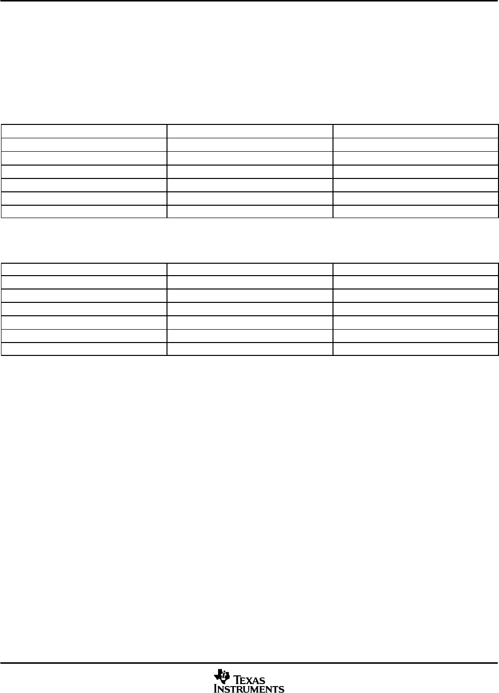
Table 3−7. TMS320VC5509A Serial Port1 Signal Routing
PIN SIGNAL MCBSP1 (00)
MMC/SD1 (01)
S10 McBSP1.CLKR MMC1.CMD
S11 McBSP1.DR MMC1.DAT1
S12 McBSP1.FSR MMC1.DAT2
S13 McBSP1.DX MMC1.CLK
S14 McBSP1.CLKX MMC1.DAT0
S15 McBSP1.FSX MMC1.DAT3
Represents the Serial Port1 Mode bits of the External Bus Selection Register.
Table 3−8. TMS320VC5509A Serial Port2 Signal Routing
PIN SIGNAL MCBSP2 (00)
MMC/SD2 (01)
S20 McBSP2.CLKR MMC2.CMD
S21 McBSP2.DR MMC2.DAT1
S22 McBSP2.FSR MMC2.DAT2
S23 McBSP2.DX MMC2.CLK
S24 McBSP2.CLKX MMC2.DAT0
S25 McBSP2.FSX MMC2.DAT3
Represents the Serial Port2 Mode bits of the External Bus Selection Register.
PREVIOUS89101112131415161718192021NEXT