Freelance Electronics Components Distributor
Closed Dec 25th-26th
800-300-1968
We Stock Hard to Find Parts

TMS320VC5509APGE

Part # TMS320VC5509APGE
Description FIXED POINT DIGITAL SIGNAL PROCESSOR -DSP, 32 BIT, 200MHZ
Category IC
Availability Out of Stock
Qty 0
Qty Price
1 + $22.73692


Technical Document


DISCLAIMER: The information provided herein is solely for informational purposes. Customers must be aware of the suitability of this product for their application, and consider that variable factors such as Manufacturer, Product Category, Date Codes, Pictures and Descriptions may differ from available inventory.

Functional Overview
31
November 2002 − Revised January 2005 SPRS205D
3 Functional Overview
The following functional overview is based on the block diagram in Figure 3−1.
7/8
USB PLL
5
Number of pins determined by package type.
Figure 3−1. Block Diagram of the TMS320VC5509A
Functional Overview
32
November 2002 − Revised January 2005SPRS205D
3.1 Memory
The 5509A supports a unified memory map (program and data accesses are made to the same physical
space). The total on-chip memory is 320K bytes (128K 16-bit words of RAM and 32K 16-bit words of ROM).
3.1.1 On-Chip Dual-Access RAM (DARAM)
The DARAM is located in the byte address range 000000h−00FFFFh and is composed of eight blocks of
8K bytes each (see Table 3−1). Each DARAM block can perform two accesses per cycle (two reads, two
writes, or a read and a write). DARAM can be accessed by the internal program, data, or DMA buses. The
HPI can only access the first four (32K bytes) DARAM blocks.
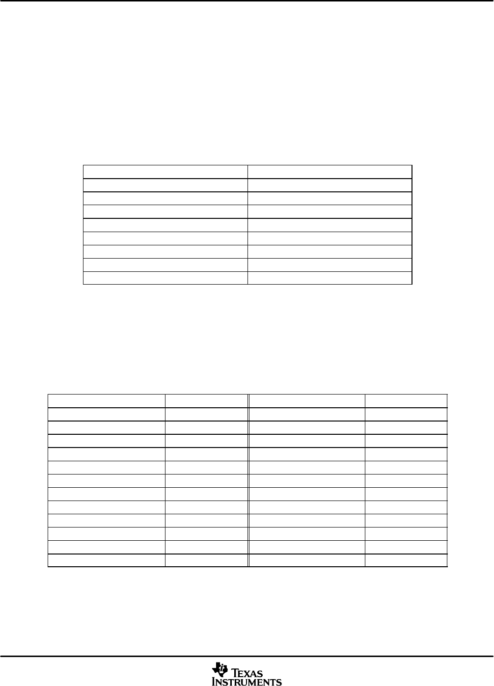
Table 3−1. DARAM Blocks
BYTE ADDRESS RANGE MEMORY BLOCK
000000h − 001FFFh DARAM 0 (HPI accessible)
002000h − 003FFFh DARAM 1 (HPI accessible)
004000h − 005FFFh DARAM 2 (HPI accessible)
006000h − 007FFFh DARAM 3 (HPI accessible)
008000h − 009FFFh DARAM 4
00A000h − 00BFFFh DARAM 5
00C000h − 00DFFFh DARAM 6
00E000h − 00FFFFh DARAM 7
First 192 bytes are reserved for Memory-Mapped Registers (MMRs).
3.1.2 On-Chip Single-Access RAM (SARAM)
The SARAM is located at the byte address range 010000h−03FFFFh and is composed of 24 blocks of 8K bytes
each (see Table 3−2). Each SARAM block can perform one access per cycle (one read or one write). SARAM
can be accessed by the internal program, data, or DMA buses.
Table 3−2. SARAM Blocks
BYTE ADDRESS RANGE MEMORY BLOCK BYTE ADDRESS RANGE MEMORY BLOCK
010000h − 011FFFh SARAM 0 028000h − 029FFFh SARAM 12
012000h − 013FFFh SARAM 1 02A000h − 02BFFFh SARAM 13
014000h − 015FFFh SARAM 2 02C000h − 02DFFFh SARAM 14
016000h − 017FFFh SARAM 3 02E000h − 02FFFFh SARAM 15
018000h − 019FFFh SARAM 4 030000h − 031FFFh SARAM 16
01A000h − 01BFFFh SARAM 5 032000h − 033FFFh SARAM 17
01C000h − 01DFFFh SARAM 6 034000h − 035FFFh SARAM 18
01E000h − 01FFFFh SARAM 7 036000h − 037FFFh SARAM 19
020000h − 021FFFh SARAM 8 038000h − 039FFFh SARAM 20
022000h − 023FFFh SARAM 9 03A000h − 03BFFFh SARAM 21
024000h − 025FFFh SARAM 10 03C000h − 03DFFFh SARAM 22
026000h − 027FFFh SARAM 11 03E000h − 03FFFFh SARAM 23
Functional Overview
33
November 2002 − Revised January 2005 SPRS205D
3.1.3 On-Chip Read-Only Memory (ROM)
The one-wait-state ROM is located at the byte address range FF0000h−FFFFFFh. The ROM is composed
of one block of 32K bytes and two 16K-byte blocks, for a total of 64K bytes of ROM. The ROM address space
can be mapped by software to the external memory or to the internal ROM.
NOTE: Customers can arrange to have the 5509A ROM programmed with contents unique
to any particular application. Contact your local Texas Instruments representative for more
information on custom ROM programming.
The standard 5509A device includes a bootloader program resident in the ROM. When the MPNMC bit field
of the ST3 status register is set through software, the on-chip ROM is disabled and not present in the memory
map, and byte address range FF0000h−FFFFFFh is directed to external memory space. A hardware reset
always clears the MPNMC bit, so it is not possible to disable the ROM at reset. However, the software reset
instruction does not affect the MPNMC bit. All three ROM blocks can be accessed by the program, data, or
DMA buses. The first 16-bit word access to ROM requires three cycles. Subsequent accesses require two
cycles per 16-bit word.
3.1.4 Memory Map
The 5509A provides 16M bytes of total memory space composed of on-chip RAM, on-chip ROM, and external
memory space supporting a variety of memory types. The on-chip, dual-access RAM allows two accesses
to a given block during the same cycle. The 5509A supports 8 blocks of 8K bytes of dual-access RAM. The
on-chip, single-access RAM allows one access to a given block per clock cycle. The 5509A supports
24 blocks of 8K byte of single-access RAM.
The remainder of the memory map is external space that is divided into four spaces. Each space has a chip
enable decode signal (called CE) that indicates an access to the selected space. The External Memory
Interface (EMIF) supports access to asynchronous memories such as SRAM and Flash, and synchronous
DRAM.
PREVIOUS4567891011121314151617NEXT