TMS320F2810, TMS320F2812
DIGITAL SIGNAL PROCESSORS
SPRS174B – APRIL 2001 – REVISED SEPTEMBER 2001
98
POST OFFICE BOX 1443 • HOUSTON, TEXAS 77251–1443
absolute maximum ratings over operating free-air temperature ranges (unless otherwise noted)
†
Supply voltage range, V
DD
, PLLV
CCA
, V
DDO
, and V
CCA
(see Note 1) – 0.3 V to 4.6 V. . . . . . . . . . . . . . . . . .
Supply voltage range, CV
DD
– 0.5 V to 2 V. . . . . . . . . . . . . . . . . . . . . . . . . . . . . . . . . . . . . . . . . . . . . . . . . . . . . . . .
V
CCP
range – 0.3 V to 3.6 V. . . . . . . . . . . . . . . . . . . . . . . . . . . . . . . . . . . . . . . . . . . . . . . . . . . . . . . . . . . . . . . . . . . . .
Input voltage range, V
IN
– 0.3 V to 4.6 V. . . . . . . . . . . . . . . . . . . . . . . . . . . . . . . . . . . . . . . . . . . . . . . . . . . . . . . . . .
Output voltage range, V
O
– 0.3 V to 4.6 V. . . . . . . . . . . . . . . . . . . . . . . . . . . . . . . . . . . . . . . . . . . . . . . . . . . . . . . . .
Output voltage range,V
O
– 0.3 V to 4.6 V. . . . . . . . . . . . . . . . . . . . . . . . . . . . . . . . . . . . . . . . . . . . . . . . . . . . . . . . . .
Input clamp current, I
IK
(V
IN
< 0 or V
IN
> V
CC
) ± 20 mA. . . . . . . . . . . . . . . . . . . . . . . . . . . . . . . . . . . . . . . . . . . . .
Output clamp current, I
OK
(V
O
< 0 or V
O
> V
CC
) ± 20 mA. . . . . . . . . . . . . . . . . . . . . . . . . . . . . . . . . . . . . . . . . . . .
Operating free-air temperature ranges, T
A
: A version – 40°C to 85°C. . . . . . . . . . . . . . . . . . . . . . . . . . . . . . . . . .
S version – 40°C to 125°C. . . . . . . . . . . . . . . . . . . . . . . . . . . . . . . .
Junction temperature range, T
J
– 40°C to 150°C. . . . . . . . . . . . . . . . . . . . . . . . . . . . . . . . . . . . . . . . . . . . . . . . . . .
Storage temperature range, T
stg
– 65°C to 150°C. . . . . . . . . . . . . . . . . . . . . . . . . . . . . . . . . . . . . . . . . . . . . . . . . .
†
Clamp current stresses beyond those listed under “absolute maximum ratings” may cause permanent damage to the device. These are stress
ratings only, and functional operation of the device at these or any other conditions beyond those indicated under “recommended operating
conditions” is not implied. Exposure to absolute-maximum-rated conditions for extended periods may affect device reliability.
NOTE 1: All voltage values are with respect to V
SS
.
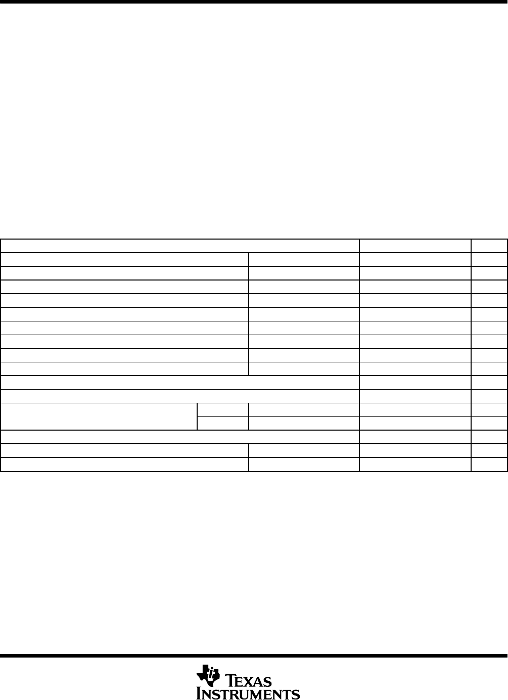
recommended operating conditions
‡§
MIN NOM MAX UNIT
V
DD
/V
DDO
Supply voltage V
DDO
= V
DD
± 0.3 V 3 3.3 3.6 V
CV
DD
Device supply voltage, CPU/core 1.65 1.8 1.95 V
V
SS
Supply ground 0 0 0 V
PLLV
CCA
PLL supply voltage 3 3.3 3.6 V
V
CCA
¶
ADC supply voltage 3 3.3 3.6 V
V
CCP
Flash programming supply voltage 3 3.3 3.6 V
f
CLKOUT
Device clock frequency (system clock) 2 150 MHz
V
IH
High-level input voltage All inputs 2 V
V
IL
Low-level input voltage All inputs 0.8 V
I
OH
High-level output source current, V
OH
= 2.4 V – 2 mA
I
OL
Low-level output sink current, V
OL
= V
OL
MAX 2 mA
A version – 40 85 °C
T
A
Free-air temperature
S version
– 40 125 °C
T
J
Junction temperature – 40 25 150 °C
N
f
Flash endurance for the array (Write/erase cycles) – 40°C to 85°C TBD cycles
N
OTP
OTP endurance for the array (Write cycles) – 40°C to 85°C 1 cycles
‡
Refer to the mechanical data package page for thermal resistance values, Θ
JA
(junction-to-ambient) and Θ
JC
(junction-to-case).
§
The drive strength of the EVA PWM pins and the EVB PWM pins are not identical.
¶
V
CCA
should not exceed V
DD
by 0.3 V.
PR
DU
T PREVIEW


