TMS320F2810, TMS320F2812
DIGITAL SIGNAL PROCESSORS
SPRS174B – APRIL 2001 – REVISED SEPTEMBER 2001
10
POST OFFICE BOX 1443 • HOUSTON, TEXAS 77251–1443
pin functions (continued)
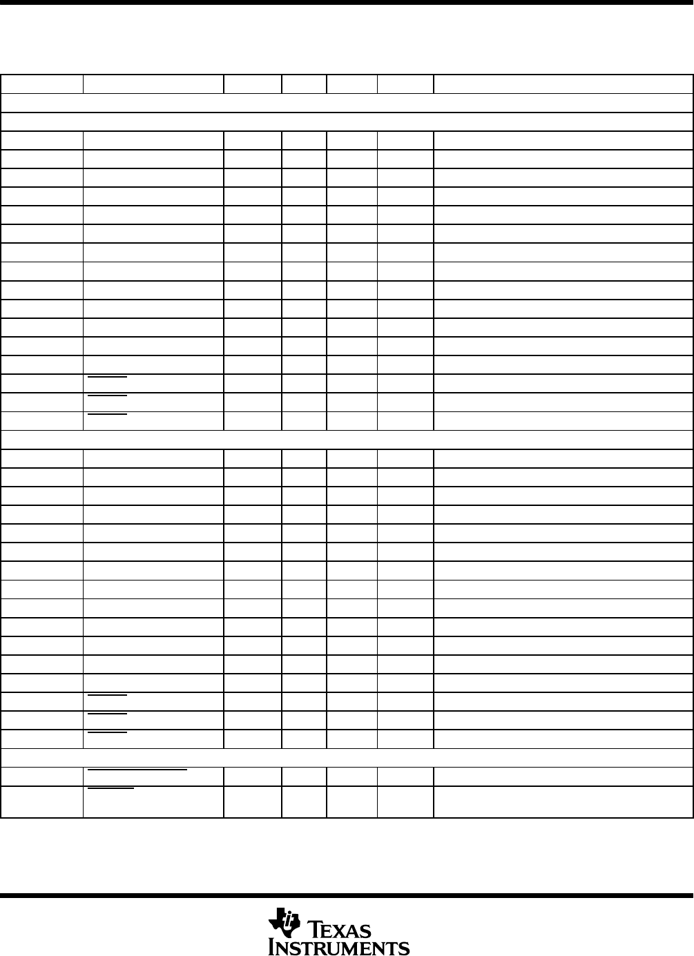
Table 2. Signal Descriptions (Continued)
GPIO PERIPHERAL SIGNAL PIN NO. I/O/Z DRIVE PU/PD
†
DESCRIPTION
GPIO OR PERIPHERAL SIGNALS
GPIOA OR EVA SIGNALS
GPIOA0 PWM1 (O) I/O/Z PU GPIO or PWM Output Pin #1
GPIOA1 PWM2 (O) I/O/Z PU GPIO or PWM Output Pin #2
GPIOA2 PWM3 (O) I/O/Z PU GPIO or PWM Output Pin #3
GPIOA3 PWM4 (O) I/O/Z PU GPIO or PWM Output Pin #4
GPIOA4 PWM5 (O) I/O/Z PU GPIO or PWM Output Pin #5
GPIOA5 PWM6 (O) I/O/Z PU GPIO or PWM Output Pin #6
GPIOA6 T1PWM_T1CMP (I) I/O/Z PU GPIO or Timer 1 Output
GPIOA7 T2PWM_T2CMP (I) I/O/Z PU GPIO or Timer 2 Output
GPIOA8 CAP1_QEP1 (I) I/O/Z PU GPIO or Capture Input #1
GPIOA9 CAP2_QEP2 (I) I/O/Z PU GPIO or Capture Input #2
GPIOA10 CAP3_QEPI1 (I) I/O/Z PU GPIO or Capture Input #3
GPIOA11 TDIRA (I) I/O/Z PU GPIO or Timer Direction
GPIOA12 TCLKINA (I) I/O/Z PU GPIO or Timer Clock Input
GPIOA13 C1TRIP (I) I/O/Z PU GPIO or Compare 1 Output Trip
GPIOA14 C2TRIP (I) I/O/Z PU GPIO or Compare 2 Output Trip
GPIOA15 C3TRIP (I) I/O/Z PU GPIO or Compare 3 Output Trip
GPIOB OR EVB SIGNALS
GPIOB0 PWM7 (O) I/O/Z PU GPIO or PWM Output Pin #7
GPIOB1 PWM8 (O) I/O/Z PU GPIO or PWM Output Pin #8
GPIOB2 PWM9 (O) I/O/Z PU GPIO or PWM Output Pin #9
GPIOB3 PWM10 (O) I/O/Z PU GPIO or PWM Output Pin #10
GPIOB4 PWM11 (O) I/O/Z PU GPIO or PWM Output Pin #11
GPIOB5 PWM12 (O) I/O/Z PU GPIO or PWM Output Pin #12
GPIOB6 T3PWM_T3CMP (I) I/O/Z PU GPIO or Timer 3 Output
GPIOB7 T4PWM_T4CMP (I) I/O/Z PU GPIO or Timer 4 Output
GPIOB8 CAP4_QEP3 (I) I/O/Z PU GPIO or Capture Input #4
GPIOB9 CAP5_QEP4 (I) I/O/Z PU GPIO or Capture Input #5
GPIOB10 CAP6_QEPI2 (I) I/O/Z PU GPIO or Capture Input #6
GPIOB11 TDIRB (I) I/O/Z PU GPIO or Timer Direction
GPIOB12 TCLKINB (I) I/O/Z PU GPIO or Timer Clock Input
GPIOB13 C4TRIP (I) I/O/Z PU GPIO or Compare 4 Output Trip
GPIOB14 C5TRIP (I) I/O/Z PU GPIO or Compare 5 Output Trip
GPIOB15 C6TRIP (I) I/O/Z PU GPIO or Compare 6 Output Trip
GPIOD OR EVA SIGNALS
GPIOD0 T1CTRIP_PDPINTA (I) I/O/Z PU Timer 1 Compare Output Trip
GPIOD1 T2CTRIP/EVASOC (I) I/O/Z PU Timer 2 Compare Output Trip or External ADC
Start-of-Conversion EV-A
†
PU = pin has internal pullup; PD = pin has internal pulldown
PR
DU
T PREVIEW


