Freelance Electronics Components Distributor
Closed Dec 25th-26th
800-300-1968
We Stock Hard to Find Parts

TMS320F2812PGFS

Part # TMS320F2812PGFS
Description MIXED-SIGNAL 28X DSPS EXTENDED TEMP
Category IC
Availability Out of Stock
Qty 0
Qty Price
1 + $17.62840


Technical Document


DISCLAIMER: The information provided herein is solely for informational purposes. Customers must be aware of the suitability of this product for their application, and consider that variable factors such as Manufacturer, Product Category, Date Codes, Pictures and Descriptions may differ from available inventory.

TMS320F2810, TMS320F2812
DIGITAL SIGNAL PROCESSORS
SPRS174B APRIL 2001 REVISED SEPTEMBER 2001
85
POST OFFICE BOX 1443 HOUSTON, TEXAS 772511443
GPIO mux
The GPIO Mux registers, are used to select the operation of shared pins on the F2810 and F2812 devices. The
pins can be individually selected to operate as Digital I/O or connected to Peripheral I/O signals (via the
GPxMUX registers). If selected for Digital I/O mode, registers are provided to configure the pin direction (via
the GPxDIR registers) and to qualify the input signal to remove unwanted noise (via the GPxQUAL) registers).
Table 60 lists the GPIO Mux Registers.
Table 60. GPIO Mux Registers
†‡§
NAME ADDRESS SIZE (x16) REGISTER DESCRIPTION
GPAMUX 0x000070C0 1 GPIO A Mux Control Register
GPADIR 0x000070C1 1 GPIO A Direction Control Register
GPAQUAL 0x000070C2 1 GPIO A Input Qualification Control Register
reserved 0x000070C3 1
GPBMUX 0x000070C4 1 GPIO B Mux Control Register
GPBDIR 0x000070C5 1 GPIO B Direction Control Register
GPBQUAL 0x000070C6 1 GPIO B Input Qualification Control Register
reserved 0x000070C7 1
reserved 0x000070C8 1
reserved 0x000070C9 1
reserved 0x000070CA 1
reserved 0x000070CB 1
GPDMUX 0x000070CC 1 GPIO D Mux Control Register
GPDDIR 0x000070CD 1 GPIO D Direction Control Register
GPDQUAL 0x000070CE 1 GPIO D Input Qualification Control Register
reserved 0x000070CF 1
GPEMUX 0x000070D0 1 GPIO E Mux Control Register
GPEDIR 0x000070D1 1 GPIO E Direction Control Register
GPEQUAL 0x000070D2 1 GPIO E Input Qualification Control Register
reserved 0x000070D3 1
GPFMUX 0x000070D4 1 GPIO F Mux Control Register
GPFDIR 0x000070D5 1 GPIO F Direction Control Register
reserved 0x000070D6 1
reserved 0x000070D7 1
GPGMUX 0x000070D8 1 GPIO F Mux Control Register
GPGDIR 0x000070D9 1 GPIO F Direction Control Register
reserved 0x000070DA 1
reserved 0x000070DB 1
reserved 0x000070DC
0x000070DF
4
Registers that are not implemented will return undefined values and writes will be ignored.
Not all inputs will support input signal qualification.
§
These registers are EALLOW protected. This prevents spurious writes from overwriting the contents and corrupting the system.
PR
O
DU
C
T PREVIEW
TMS320F2810, TMS320F2812
DIGITAL SIGNAL PROCESSORS
SPRS174B APRIL 2001 REVISED SEPTEMBER 2001
86
POST OFFICE BOX 1443 HOUSTON, TEXAS 772511443
GPIO mux (continued)
If configured for Digital I/O mode, additional registers are provided for setting individual I/O signals (via the
GPxSET registers), for clearing individual I/O signals (via the GPxCLEAR registers), for toggling individual I/O
signals (via the GPxTOGGLE registers), or for reading/writing to the individual I/O signals (via the GPxDAT
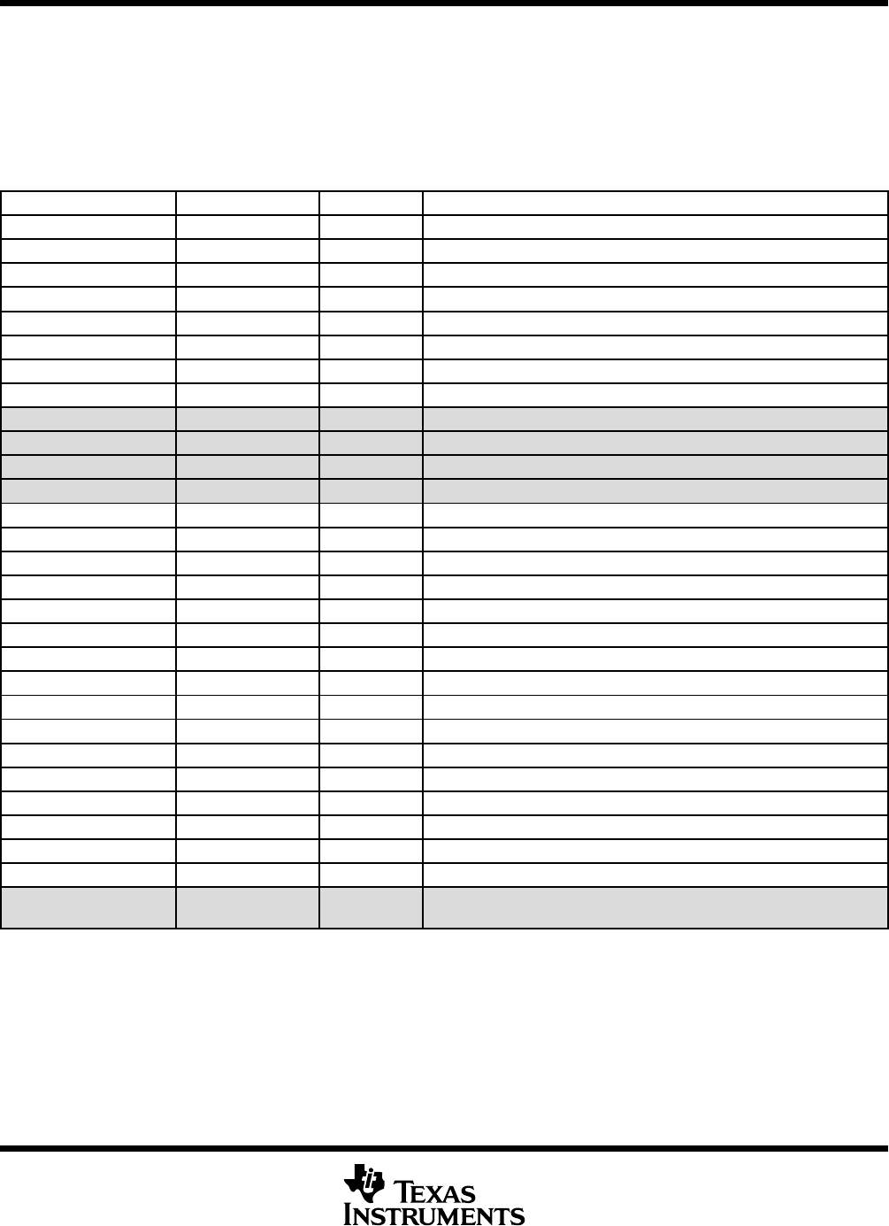
registers). Table 61 lists the GPIO Data Registers.
Table 61. GPIO Data Registers
†‡
NAME ADDRESS SIZE (x16) REGISTER DESCRIPTION
GPADAT 0x000070E0 1 GPIO A Data Register
GPASET 0x000070E1 1 GPIO A Set Register
GPACLEAR 0x000070E2 1 GPIO A Clear Register
GPATOGGLE 0x000070E3 1 GPIO A Toggle Register
GPBDAT 0x000070E4 1 GPIO B Data Register
GPBSET 0x000070E5 1 GPIO B Set Register
GPBCLEAR 0x000070E6 1 GPIO B Clear Register
GPBTOGGLE 0x000070E7 1 GPIO B Toggle Register
reserved 0x000070E8 1
reserved 0x000070E9 1
reserved 0x000070EA 1
reserved 0x000070EB 1
GPDDAT 0x000070EC 1 GPIO D Data Register
GPDSET 0x000070ED 1 GPIO D Set Register
GPDCLEAR 0x000070EE 1 GPIO D Clear Register
GPDTOGGLE 0x000070EF 1 GPIO D Toggle Register
GPEDAT 0x000070F0 1 GPIO E Data Register
GPESET 0x000070F1 1 GPIO E Set Register
GPECLEAR 0x000070F2 1 GPIO E Clear Register
GPETOGGLE 0x000070F3 1 GPIO E Toggle Register
GPFDAT 0x000070F4 1 GPIO F Data Register
GPFSET 0x000070F5 1 GPIO F Set Register
GPFCLEAR 0x000070F6 1 GPIO F Clear Register
GPFTOGGLE 0x000070F7 1 GPIO F Toggle Register
GPGDAT 0x000070F8 1 GPIO G Data Register
GPGSET 0x000070F9 1 GPIO G Set Register
GPGCLEAR 0x000070FA 1 GPIO G Clear Register
GPGTOGGLE 0x000070FB 1 GPIO G Toggle Register
reserved 0x000070FC
0x000070FF
4
Reserved locations will return undefined values and writes will be ignored.
These registers are NOT EALLOW protected. The above registers will typically be accessed regularly by the user.
PR
O
DU
C
T PREVIEW
TMS320F2810, TMS320F2812
DIGITAL SIGNAL PROCESSORS
SPRS174B APRIL 2001 REVISED SEPTEMBER 2001
87
POST OFFICE BOX 1443 HOUSTON, TEXAS 772511443
GPIO mux (continued)
Figure 21 shows how the various register bits select the various modes of operation.
Peripheral I/O
MUX
01
MUX
10
PIN
Internal (Pullup or Pulldown)
HSPCLK (High-Speed Peripheral Clock)
Digital I/O
QUALxCLK
Boundary Off
XRS
High-Impedance
Enable (1)
High-
Impedance
Control
GPxDIR
Register Bit
GPxMUX
Register Bit
GPxQUAL
Register
GPxDAT/SET/CLEAR/TOGGLE
Register Bit(s)
Input
Qualification
Pre-Scale
Figure 21. Modes of Operation
Notes:
1. Via the GPxDAT register, the state of any PIN can be read, regardless of the operating mode.
2. Some selected input signals are, qualified by the QUALxCLK, which is a prescaled version of the
high-speed peripheral clock (HSPCLK). The GPxQUAL register specifies the qualification sampling period.
The sampling window is 6 samples wide and the output is only changed when all samples are the same
(all 0s or all 1s) as shown in Figure 22. This feature removes unwanted spikes from the input signal.
PR
O
DU
C
T PREVIEW
PREVIOUS2223242526272829303132333435NEXT