TMS320F2810, TMS320F2812
DIGITAL SIGNAL PROCESSORS
SPRS174B – APRIL 2001 – REVISED SEPTEMBER 2001
57
POST OFFICE BOX 1443 • HOUSTON, TEXAS 77251–1443
32-bit CPU-Timers 0/1/2 (continued)
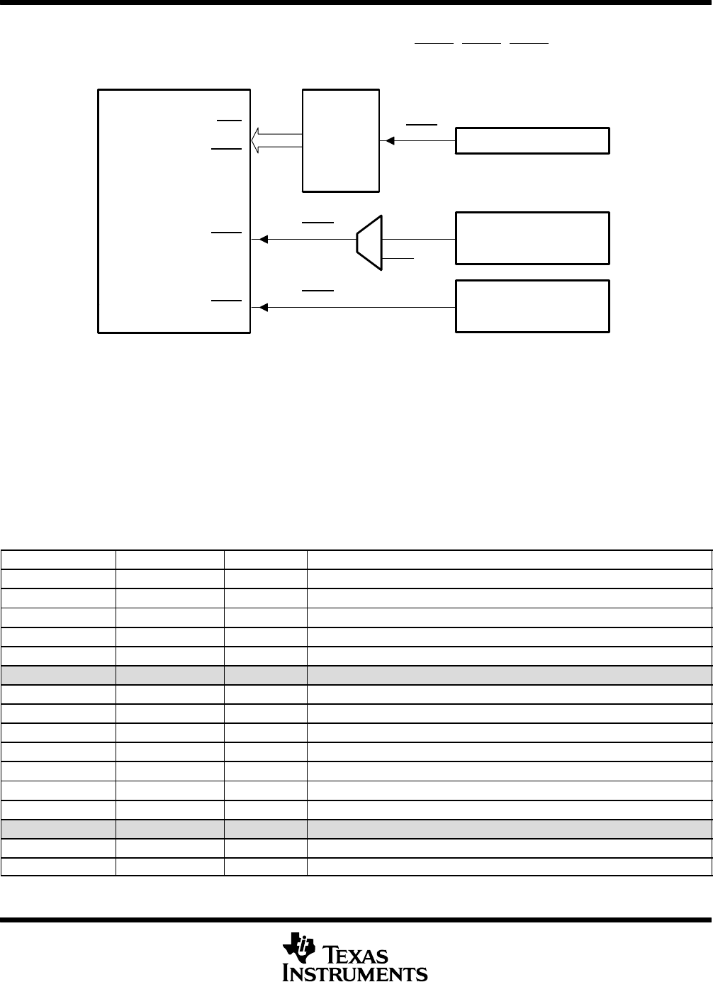
In the F2810 and F2812 devices, the timer interrupt signals (TINT0, TINT1, TINT2) are connected as shown
in Figure 13.
INT1
to
INT12
INT14
C28x
TINT2
TINT0
PIE
CPU-TIMER 0
CPU-TIMER 2
(for RTOS use)
INT13
TINT1
CPU-TIMER 1
(for RTOS use)
XINT13
NOTES: A. The timer registers are connected to the Memory Bus of the C28x processor.
B. The timing of the timers is synchronized to SYSCLKOUT of the processor clock.
Figure 13. CPU-Timer Interrupts Signals and Output Signal
The general operation of the timer is as follows: The 32-bit counter register “TIMH:TIM” is loaded with the value
in the period register “PRDH:PRD”. The counter register, decrements at the SYSCLKOUT rate of the C28x.
When the counter reaches 0, a timer interrupt output signal generates an interrupt pulse. The registers listed
in Table 43 are used to configure the timers.
Table 43. CPU-Timers 0, 1, 2 Configuration and Control Registers
NAME ADDRESS SIZE (x16) DESCRIPTION
TIMER0TIM 0x0000–0C00 1 CPU-Timer 0, Counter Register
TIMER0TIMH 0x0000–0C01 1 CPU-Timer 0, Counter Register High
TIMER0PRD 0x0000–0C02 1 CPU-Timer 0, Period Register
TIMER0PRDH 0x0000–0C03 1 CPU-Timer 0, Period Register High
TIMER0TCR 0x0000–0C04 1 CPU-Timer 0, Control Register
reserved 0x0000–0C05 1
TIMER0TPR 0x0000–0C06 1 CPU-Timer 0, Prescale Register
TIMER0TPRH 0x0000–0C07 1 CPU-Timer 0, Prescale Register High
TIMER1TIM 0x0000–0C08 1 CPU-Timer 1, Counter Register
TIMER1TIMH 0x0000–0C09 1 CPU-Timer 1, Counter Register High
TIMER1PRD 0x0000–0C0A 1 CPU-Timer 1, Period Register
TIMER1PRDH 0x0000–0C0B 1 CPU-Timer 1, Period Register High
TIMER1TCR 0x0000–0C0C 1 CPU-Timer 1, Control Register
reserved 0x0000–0C0D 1
TIMER1TPR 0x0000–0C0E 1 CPU-Timer 1, Prescale Register
TIMER1TPRH 0x0000–0C0F 1 CPU-Timer 1, Prescale Register High
PR
DU
T PREVIEW


