TMS320F2810, TMS320F2812
DIGITAL SIGNAL PROCESSORS
SPRS174B – APRIL 2001 – REVISED SEPTEMBER 2001
49
POST OFFICE BOX 1443 • HOUSTON, TEXAS 77251–1443
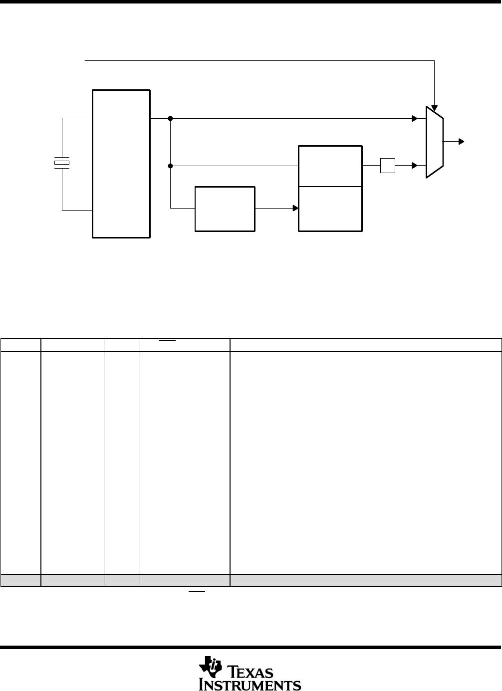
OSC and PLL block
The OSC and PLL block on the F2810 and F2812 will use a zero-pin Phase-Locked Loop (ZPLL). Figure 10
shows the implemented features and relevant signals.
XTAL2
XTAL1/CLKIN
On-Chip
Oscillator
(OSC)
4-bit
PLL Select
PLL
Bypass
/2
XPLLDIS
PLL
OSCCLK
Figure 10. OSC and PLL Block
The OSC circuit enables a crystal to be attached to the F2810 and F2812 devices using the X1 and X2 pins.
If a crystal is not used, then an external oscillator can be directly connected to the XCLKIN pin and the X2 pin
is left unconnected. The oscillator input range is 20 MHz to 35 MHz.
Table 36. PLLCR Register Bit Definitions
BIT(S) NAME TYPE XRS RESET
†
DESCRIPTION
3:0 DIV R/W 0,0,0,0 These bits set the PLL clocking ratio. The range of values should be between
(x 1.0) to (x 10.0). The scale between these values should be as linear as
possible:
0000 x 0.5 PLL bypassed but enabled
CLKIN = OSCCLK / 2
0001 x 1.0 PLL connected
CLKIN (OSCCLK * 1.0) / 2
0010 x 2.0 CLKIN = (OSCCLK * 2.0) / 2
0011 x 3.0 CLKIN = (OSCCLK * 3.0) / 2
0100 x 4.0 CLKIN = (OSCCLK * 4.0) / 2
0101 x 5.0 CLKIN = (OSCCLK * 5.0) / 2
0110 x 6.0 CLKIN = (OSCCLK * 6.0) / 2
0111 x 7.0 CLKIN = (OSCCLK * 7.0) / 2
1000 x 8.0 CLKIN = (OSCCLK * 8.0) / 2
1001 x 9.0 CLKIN = (OSCCLK * 9.0) / 2
1010 x 10.0 CLKIN = (OSCCLK * 10.0) / 2
1011 spare
1100 spare
1101 spare
1110 spare
1111 spare
15:4 reserved R=0 0:0
†
The PLLCR register is reset to a known state by the XRS
reset line. If a reset is issued by the debugger, the PLL clocking ratio is not changed.
PR
DU
T PREVIEW


