Freelance Electronics Components Distributor
Closed Dec 25th-26th
800-300-1968
We Stock Hard to Find Parts

TMS320F2812PGFS

Part # TMS320F2812PGFS
Description MIXED-SIGNAL 28X DSPS EXTENDED TEMP
Category IC
Availability Out of Stock
Qty 0
Qty Price
1 + $17.62840


Technical Document


DISCLAIMER: The information provided herein is solely for informational purposes. Customers must be aware of the suitability of this product for their application, and consider that variable factors such as Manufacturer, Product Category, Date Codes, Pictures and Descriptions may differ from available inventory.

TMS320F2810, TMS320F2812
DIGITAL SIGNAL PROCESSORS
SPRS174B APRIL 2001 REVISED SEPTEMBER 2001
43
POST OFFICE BOX 1443 HOUSTON, TEXAS 772511443
external interrupts (continued)
The masked interrupts, XINT1/2 and NMI, also contain a 16-bit up-counter register that is reset to 0x0000
whenever an interrupt edge is detected. This counter can be used to accurately time stamp the occurrence of
the interrupt. Table 30 shows the bit definitions of the XINT1/2CTR and XNMICTR registers.
Table 30. XINT1/2CTR and XNMICTR Registers Bit Definitions
BITS NAME TYPE RESET DESCRIPTION
15:0 INTCTR R 0:0 This is a free running 16-bit up-counter that is clocked at the SYSCLKOUT rate. The
counter value is reset to 0x0000 when a valid interrupt edge is detected and then continues
counting until the next valid interrupt edge is detected. The counter must only be reset by
the selected POLARITY edge as selected in the respective interrupt control register. When
the interrupt is disabled, the counter will stop. The counter is a free-running counter and
will wrap around to zero when the max value is reached. The counter is a read only register
and can only be reset to zero by a valid interrupt edge or by reset.
PR
O
DU
C
T PREVIEW
TMS320F2810, TMS320F2812
DIGITAL SIGNAL PROCESSORS
SPRS174B APRIL 2001 REVISED SEPTEMBER 2001
44
POST OFFICE BOX 1443 HOUSTON, TEXAS 772511443
system control
This section describes the F2810 and F2812 oscillator, PLL and clocking mechanisms, the watchdog function
and the low power modes. Figure 9 shows the various clock and reset domains in the F2810 and F2812 devices
that will be discussed.
HSPCLK
PLL
X1/XCLKIN
X2
Power
Modes
Control
Watchdog
Block
C28x
CPU
Peripheral Bus
Low-Speed Peripherals
SCI-A/B, SPI, McBSP
Peripheral
Registers
High-Speed Peripherals
EV-A/B
High-Speed Prescaler
Low-Speed Prescaler
Clock Enables
GPIO
MUX
System
Control
Registers
Peripheral
Registers
XPLLDIS
ADC
Registers
12-Bit ADC
16 ADC Inputs
HSPCLK
LSPCLK
I/O
I/O
Peripheral Reset
SYSCLKOUT
XRS
Reset
GPIOs
eCAN
Peripheral
Registers
I/O
OSC
CLKIN
Figure 9. Clock and Reset Domains
PR
O
DU
C
T PREVIEW
TMS320F2810, TMS320F2812
DIGITAL SIGNAL PROCESSORS
SPRS174B APRIL 2001 REVISED SEPTEMBER 2001
45
POST OFFICE BOX 1443 HOUSTON, TEXAS 772511443
system control (continued)
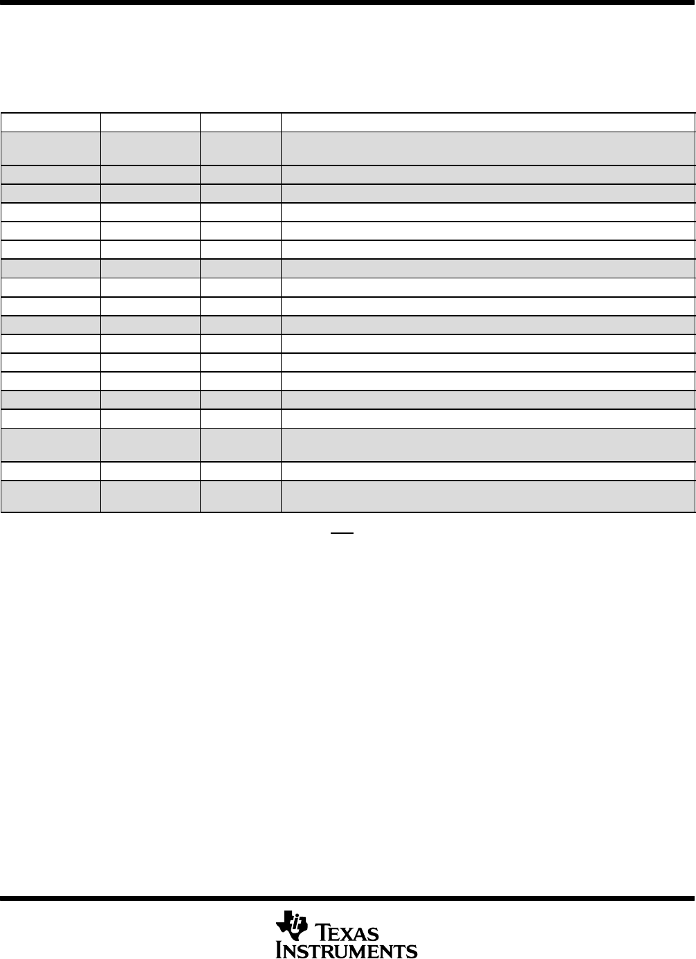
The PLL, clocking, watchdog and low-power modes, are controlled by the registers listed in Table 31.
Table 31. PLL, Clocking, Watchdog, and Low-Power Mode Registers
NAME ADDRESS SIZE (x16) DESCRIPTION
reserved 0x00007010
0x00007017
8
reserved 0x00007018 1
reserved 0x00007019 1
HISPCP 0x0000701A 1 High-Speed Peripheral Clock Prescaler Register for HSPCLK clock
LOSPCP 0x0000701B 1 Low-Speed Peripheral Clock Prescaler Register for HSPCLK clock
PCLKCR 0x0000701C 1 Peripheral Clock Control Register
reserved 0x0000701D 1
LPMCR0 0x0000701E 1 Low Power Mode Control Register 0
LPMCR1 0x0000701F 1 Low Power Mode Control Register 1
reserved 0x00007020 1
PLLCR 0x00007021 1 PLL Control Register
SCSR 0x00007022 1 System Control & Status Register
WDCNTR 0x00007023 1 Watchdog Counter Register
reserved 0x00007024 1
WDKEY 0x00007025 1 Watchdog Reset Key Register
reserved 0x00007026
0x00007028
3
WDCR 0x00007029 1 Watchdog Control Register
reserved 0x0000702A
0x0000702F
6
All of the above registers can only be accessed, by executing the EALLOW instruction.
The PLL control register (PLLCR) is reset to a known state by the XRS
signal only.
PR
O
DU
C
T PREVIEW
PREVIOUS89101112131415161718192021NEXT