Closed Dec 25th-26th
800-300-1968
We Stock Hard to Find Parts
My Account
|
My Orders
|
My Cart
Questions?
(800) 300-1968
Register
(current)
My Account
(current)
My Orders
(current)
My Cart
(current)
Categories
(current)
Manufacturers
Request a Quote
Sell Your Excess
Consignment
Quality Assurance
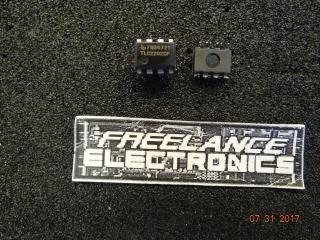
TLC2274MFKB
Part #
TLC2274MFKB
Description
OP Amp Quad GP R-R O/P ±8V/16V 20-Pin LCCC Tube - Rail/Tub
Category
IC
Availability
In Stock
Qty
2
Qty
Price
1 +
$28.58858
Manufacturer
Available
Qty
Texas Instruments
Date Code: 9645
Freelance Stock:
2
Ships Immediately
Add to Cart
Related Items
Texas Instruments
IC
TLC2201AC
Texas Instruments
IC
TLC2201AMJG
$6.81850
Texas Instruments
IC
TLC2202CP
$7.12378
Texas Instruments
IC
TLC2272AIDR
$1.12506
Texas Instruments
IC
TLC2272AMD
$1.35006
Texas Instruments
IC
TLC2272CDR
$0.88608