Freelance Electronics Components Distributor
Closed Dec 25th-26th
800-300-1968
We Stock Hard to Find Parts

TLC193MJGB

Part # TLC193MJGB
Description Comparator Dual 16V 8-Pin CDIP Tube
Category IC
Availability In Stock
Qty 8
Qty Price
1 - 1 $13.73878
2 - 3 $10.92858
4 - 5 $10.30409
6 - 6 $9.57552
7 + $8.53470
Manufacturer Available Qty
Texas Instruments
Date Code: 8820
  • Shipping Freelance Stock: 8
    Ships Immediately


Technical Document


DISCLAIMER: The information provided herein is solely for informational purposes. Customers must be aware of the suitability of this product for their application, and consider that variable factors such as Manufacturer, Product Category, Date Codes, Pictures and Descriptions may differ from available inventory.

 
    
SLCS115E DECEMBER 1986 REVISED JULY 2003
7
POST OFFICE BOX 655303 DALLAS, TEXAS 75265
POST OFFICE BOX 1443
HOUSTON, TEXAS 772511443
switching characteristics, V
DD
= 5 V, T
A
= 25°C (see Figure 3)
PARAMETER TEST CONDITIONS
TLC393C, TLC393I
TLC393Q, TLC193M,
TLC393M
UNIT
MIN TYP MAX
Overdrive = 2 mV 4.5
f10kH
Overdrive = 5 mV 2.5
t
PLH
Propagation delay time, low-to-high-level output
f = 10 kHz,
C
L
=15
p
F
Overdrive = 10 mV 1.7
µs
t
PLH
Pro agation
delay
time,
low to high level
out ut
C
L
=
15
p
F
Overdrive = 20 mV 1.2
µs
Overdrive = 40 mV 1.1
V
I
= 1.4-V step at IN+ 1.1
Overdrive = 2 mV 3.6
f10kH
Overdrive = 5 mV 2.1
t
PHL
Propagation delay time, high-to-low-level output
f = 10 kHz,
C
L
=15
p
F
Overdrive = 10 mV 1.3
µs
t
PHL
Pro agation
delay
time,
high to low level
out ut
C
L
=
15
p
F
Overdrive = 20 mV 0.85
µs
Overdrive = 40 mV 0.55
V
I
= 1.4-V step at IN+ 0.10
t
f
Fall time, output
f = 10 kHz,
C
L
= 15 pF
Overdrive = 50 mV 22 ns
PARAMETER MEASUREMENT INFORMATION
The TLC393 contains a digital output stage which, if held in the linear region of the transfer curve, can cause
damage to the device. Conventional operational amplifier/comparator testing incorporates the use of a servo
loop that is designed to force the device output to a level within this linear region. Since the servo-loop method
of testing cannot be used, the following alternatives for testing parameters such as input offset voltage,
common-mode rejection ratio, etc., are suggested.
To verify that the input offset voltage falls within the limits specified, the limit value is applied to the input as shown
in Figure 1(a). With the noninverting input positive with respect to the inverting input, the output should be high.
With the input polarity reversed, the output should be low.
A similar test can be made to verify the input offset voltage at the common-mode extremes. The supply voltages
can be slewed as shown in Figure 1(b) for the V
ICR
test, rather than changing the input voltages, to provide
greater accuracy.
+
5 V
Applied V
IO
Limit
V
O
+
1 V
Applied V
IO
Limit
V
O
4 V
(a) V
IO
WITH V
IC
= 0 V (b) V
IO
WITH V
IC
= 4 V
5.1 k 5.1 k
Figure 1. Method for Verifying That Input Offset Voltage Is Within Specified Limits
 
    
SLCS115D DECEMBER 1986 REVISED JULY 2003
8
POST OFFICE BOX 655303 DALLAS, TEXAS 75265
POST OFFICE BOX 1443
HOUSTON, TEXAS 772511443
PARAMETER MEASUREMENT INFORMATION
A close approximation of the input offset voltage can be obtained by using a binary search method to vary the
differential input voltage while monitoring the output state. When the applied input voltage differential is equal,
but opposite in polarity, to the input offset voltage, the output changes states.
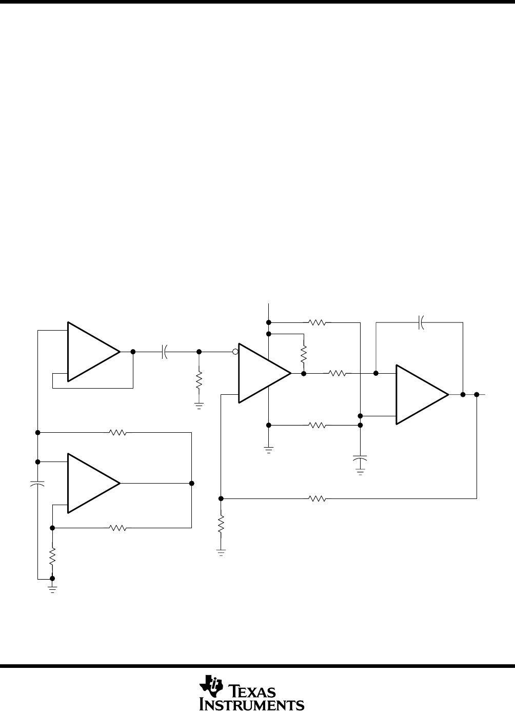
Figure 2 illustrates a practical circuit for direct dc measurement of input offset voltage that does not bias the
comparator in the linear region. The circuit consists of a switching-mode servo loop in which U1A generates
a triangular waveform of approximately 20-mV amplitude. U1B acts as a buffer, with C2 and R4 removing any
residual dc offset. The signal is then applied to the inverting input of the comparator under test, while the
noninverting input is driven by the output of the integrator formed by U1C through the voltage divider formed
by R9 and R10. The loop reaches a stable operating point when the output of the comparator under test has
a duty cycle of exactly 50%, which can only occur when the incoming triangle wave is sliced symmetrically or
when the voltage at the noninverting input exactly equals the input offset voltage.
The voltage divider formed by R9 and R10 provides an increase in input offset voltage by a factor of 100 to
make measurement easier. The values of R5, R8, R9, and R10 can significantly influence the accuracy of the
reading; therefore, it is suggested that their tolerance level be 1% or lower.
Measuring the extremely low values of input current requires isolation from all other sources of leakage current
and compensation for the leakage of the test socket and board. With a good picoammeter, the socket and board
leakage can be measured with no device in the socket. Subsequently, this open-socket leakage value can be
subtracted from the measurement obtained with a device in the socket to obtain the actual input current of the
device.
+
DUT
V
DD
+
+
+
C2
1 µF
R4
47 k
R5
1.8 kΩ, 1%
C3
0.68 µF
U1C
1/4 TLC274CN
U1B
1/4 TLC274CN
U1A
1/4 TLC274CN
R7
1 M
R8
1.8 kΩ, 1%
R9
10 kΩ, 1%
R1
240 k
R2
10 k
C1
0.1 µF
R3
100 k
C4
0.1 µF
Integrator
R10
100 Ω, 1%
Buffer
Triangle
Generator
V
IO
(X100)
R6
5.1 k
Figure 2. Circuit for Input Offset Voltage Measurement
 
    
SLCS115E DECEMBER 1986 REVISED JULY 2003
9
POST OFFICE BOX 655303 DALLAS, TEXAS 75265
POST OFFICE BOX 1443
HOUSTON, TEXAS 772511443
PARAMETER MEASUREMENT INFORMATION
Propagation delay time is defined as the interval between the application of an input step function and the instant
when the output reaches 50% of its maximum value. Propagation delay time, low-to-high-level output, is
measured from the leading edge of the input pulse, while propagation delay time, high-to-low-level output, is
measured from the trailing edge of the input pulse. Propagation delay time measurement at low input signal
levels can be greatly affected by the input offset voltage. The offset voltage should be balanced by the
adjustment at the inverting input (as shown in Figure 3) so that the circuit is just at the transition point. Then a
low signal, for example, 105 mV or 5 mV overdrive, causes the output to change state.
DUT
V
DD
C
L
(see
Note
A)
Pulse
Generator
10
10 Turn
1
V
1
V
1
k
50
1
µF
0.1
µF
TEST CIRCUIT
100 mV
Input
Overdrive
50%
t
PLH
100 mVInput
Overdrive
90%
50%
10%
t
f
t
PHL
Low-to-High-
Level Output
High-to-Low-
Level Output
VOLTAGE WAVEFORMS
5.1
k
Input Offset Voltage
Compensation
Adjustment
90%
t
r
10%
NOTE A: C
L
includes probe and jig capacitance.
Figure 3. Propagation Delay, Rise Time, and Fall Time Circuit and Voltage Waveforms
PREVIOUS123456789NEXT