Freelance Electronics Components Distributor
Closed Dec 25th-26th
800-300-1968
We Stock Hard to Find Parts

TIBPAL16R4-30MJB

Part # TIBPAL16R4-30MJB
Description High Performance Impact PAL Circuits 20-Pin CDIP Tube - Ra
Category IC
Availability In Stock
Qty 5
Qty Price
1 + $5.79804
Manufacturer Available Qty
Texas Instruments
Date Code: 9000
  • Shipping Freelance Stock: 3
    Ships Immediately
Texas Instruments
Date Code: 9108
  • Shipping Freelance Stock: 2
    Ships Immediately


Technical Document


DISCLAIMER: The information provided herein is solely for informational purposes. Customers must be aware of the suitability of this product for their application, and consider that variable factors such as Manufacturer, Product Category, Date Codes, Pictures and Descriptions may differ from available inventory.

TIBPAL16R4-25C, TIBPAL16R6-25C, TIBPAL16R8-25C
TIBPAL16R4-30M, TIBPAL16R6-30M, TIBPAL16R8-30M
LOW-POWER HIGH-PERFORMANCE IMPACTPAL
®
CIRCUITS
SRPS059A FEBRUARY 1984 REVISED DECEMBER 2010
13
POST OFFICE BOX 655303 DALLAS, TEXAS 75265
programming information
Texas Instruments programmable logic devices can be programmed using widely available software and
inexpensive device programmers.
Complete programming specifications, algorithms, and the latest information on hardware, software, and
firmware are available upon request. Information on programmers capable of programming Texas Instruments
programmable logic also is available, upon request, from the nearest TI field sales office or local authorized TI
distributor, by calling Texas Instruments at +1 (972) 6445580, or by visiting the TI Semiconductor Home Page
at www.ti.com/sc.
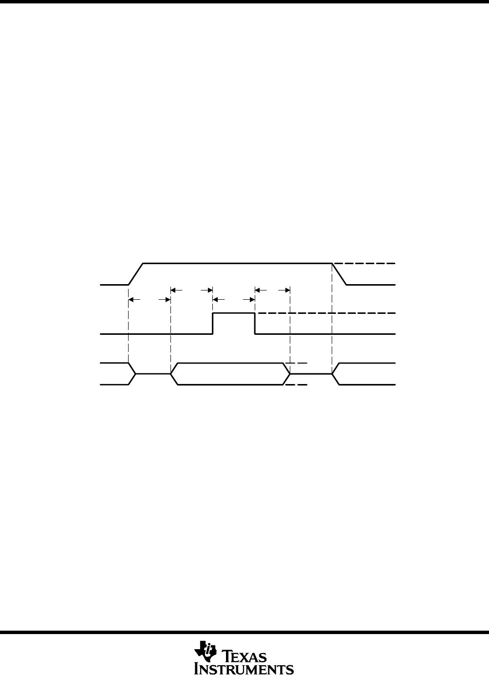
preload procedure for registered outputs (see Figure 1 and Note 3)
The output registers can be preloaded to any desired state during device testing. This permits any state to be
tested without having to step through the entire state-machine sequence. Each register is preloaded individually
by following the steps given below.
Step 1. With V
CC
at 5 V and Pin 1 at V
IL
, raise Pin 11 to V
IHH
.
Step 2. Apply either V
IL
or V
IH
to the output corresponding to the register to be preloaded.
Step 3. Pulse Pin 1, clocking in preload data.
Step 4. Remove output voltage, then lower Pin 11 to V
IL
. Preload can be verified by observing the
voltage level at the output pin.
t
d
t
su
t
w
t
d
V
IHH
V
IL
V
IL
V
OL
V
OH
V
IH
Pin 11
Pin 1
Registered I/O
Input Output
V
IH
V
IL
NOTE 3: t
d
= t
su
= t
h
= 100 ns to 1000 ns V
IHH
= 10.25 V to 10.75 V
Figure 1. Preload Waveforms
TIBPAL16R4-25C, TIBPAL16R6-25C, TIBPAL16R8-25C
TIBPAL16R4-30M, TIBPAL16R6-30M, TIBPAL16R8-30M
LOW-POWER HIGH-PERFORMANCE IMPACTPAL
®
CIRCUITS
SRPS059A FEBRUARY 1984 REVISED DECEMBER 2010
14
POST OFFICE BOX 655303 DALLAS, TEXAS 75265
power-up reset (see Figure 2)
Following power up, all registers are set high. This feature provides extra flexibility to the system designer and
is especially valuable in simplifying state-machine initialization. To ensure a valid power-up reset, it is important
that the rise of V
CC
be monotonic. Following power-up reset, a low-to-high clock transition must not occur until
all applicable input and feedback setup times are met.
1.5 V
t
su
t
pd
t
w
V
IL
V
IH
5 V
V
CC
Active-Low
Registered Output
CLK
4 V
V
OH
V
OL
1.5 V
(600 ns TYP, 1000 ns MAX)
1.5 V
This is the power-up reset time and applies to registered outputs only. The values shown are from characterization data.
This is the setup time for input or feedback.
Figure 2. Power-Up Reset Waveforms
TIBPAL16R4-25C, TIBPAL16R6-25C, TIBPAL16R8-25C
TIBPAL16R4-30M, TIBPAL16R6-30M, TIBPAL16R8-30M
LOW-POWER HIGH-PERFORMANCE IMPACTPAL
®
CIRCUITS
SRPS059A FEBRUARY 1984 REVISED DECEMBER 2010
15
POST OFFICE BOX 655303 DALLAS, TEXAS 75265
PARAMETER MEASUREMENT INFORMATION
t
dis
t
dis
t
su
S1
From Output
Under Test
Test
Point
R2
C
L
(see Note A)
LOAD CIRCUIT FOR 3-STATE OUTPUTS
t
h
Timing
Input
Data
Input
Input
In-Phase
Output
Out-of-Phase
Output
(see Note D)
t
pd
t
pd
t
pd
t
pd
VOLTAGE WAVEFORMS
SETUP AND HOLD TIMES
VOLTAGE WAVEFORMS
PROPAGATION DELAY TIMES
V
OH
V
OH
V
OL
V
OL
t
w
High-Level
Pulse
Low-Level
Pulse
Output
Control
(low-level
enabling)
Waveform 1
S1 Closed
(see Note B)
Waveform 2
S1 Open
(see Note B)
3.5 V
0.3 V
3.5 V
V
OL
V
OH
V
OH
0.3 V
0 V
t
en
t
en
VOLTAGE WAVEFORMS
ENABLE AND DISABLE TIMES, 3-STATE OUTPUTS
VOLTAGE WAVEFORMS
PULSE DURATIONS
R1
3.5 V
0.3 V
V
OL
+ 0.3 V
NOTES: A. C
L
includes probe and jig capacitance and is 50 pF for t
pd
and t
en
, 5 pF for t
dis
.
B. Waveform 1 is for an output with internal conditions such that the output is low except when disabled by the output control.
Waveform 2 is for an output with internal conditions such that the output is high except when disabled by the output control.
C. All input pulses have the following characteristics: PRR 1 MHz, t
r
= t
f
2 ns, duty cycle = 50%
D. When measuring propagation delay times of 3-state outputs from low to high, switch S1 is closed.
When measuring propagation delay times of 3-state outputs from high to low, switch S1 is open.
E. Equivalent loads may be used for testing.
1.3 V
1.3 V 1.3 V
3.5 V
0.3 V
3.5 V
0.3 V
1.3 V 1.3 V
1.3 V 1.3 V
1.3 V 1.3 V
3.5 V
0.3 V
3.5 V
0.3 V
1.3 V 1.3 V
1.3 V
1.3 V
1.3 V 1.3 V
1.3 V
1.3 V
Figure 3. Load Circuit and Voltage Waveforms
PREVIOUS123456789NEXT