Freelance Electronics Components Distributor
Closed Dec 25th-26th
800-300-1968
We Stock Hard to Find Parts

TE28F800C3BA90

Part # TE28F800C3BA90
Description NOR, Flash 512K x 16 48PinTSSOP
Category IC
Availability In Stock
Qty 375
Qty Price
1 - 78 $0.87249
79 - 157 $0.69403
158 - 236 $0.65437
237 - 315 $0.60810
316 + $0.54200
Manufacturer Available Qty
INTEL
Date Code: 0015
  • Shipping Freelance Stock: 190
    Ships Immediately
INTEL
Date Code: 0309
  • Shipping Freelance Stock: 16
    Ships Immediately
INTEL
Date Code: 0013
  • Shipping Freelance Stock: 167
    Ships Immediately
INTEL
Date Code: 0312
  • Shipping Freelance Stock: 2
    Ships Immediately


Technical Document


DISCLAIMER: The information provided herein is solely for informational purposes. Customers must be aware of the suitability of this product for their application, and consider that variable factors such as Manufacturer, Product Category, Date Codes, Pictures and Descriptions may differ from available inventory.

Intel
£
Advanced+ Boot Block Flash Memory (C3)
Datasheet 55
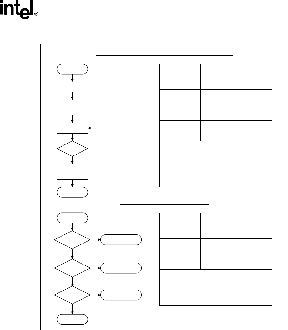
Figure 16. Block Erase Flowchart
Start
FULL ERASE STATUS CHECK PROCEDURE
Repeat for subsequent block erasur es.
Full Status regi ster check can be done after each block er ase
or after a sequence of block er asur es.
Wr ite 0xFF after the last oper ation to enter read array m ode.
SR[1,3] must be cleared before the Write State Machine will
allow further erase attem pts.
Only the Cl ear Status Register com mand clears SR[1, 3, 4, 5].
If an error is detected, clear the Status register before
attempting an erase retry or other error recovery.
No
Suspend
Erase
1
0
0
0
1
1,1
1
1
0 Yes
Suspend
Erase
Loop
0
Wri te 0x20,
Block Address
Wri te 0xD0,
Block Address
Read Status
Register
SR[7] =
Full Erase
Status Check
(if desi r ed)
Block Erase
Complete
Read Status
Register
Block Erase
Successful
SR[1] =
Block Locked
Error
BLOCK ERASE PROCEDURE
Bus
Operation
Command Comments
Wr i te
Block
Erase
Setup
Data = 0x20
Addr = Block to be er ased ( BA)
Wr i te
Erase
Confir m
Data = 0xD0
Addr = Block to be er ased ( BA)
Read None
Status R egi ster data. Toggle C E# or
OE# to update Status r egister data
Idle None
Check SR[7]:
1 = WSM ready
0= WSMbusy
Bus
Operation
Command Comments
SR[3] =
V
PP
Range
Error
SR[4,5] =
Command
Sequence Er ror
SR[5] =
Block Er ase
Error
Idle None
Check SR[3]:
1= V
PP
Range Error
Idle None
Check SR[4,5]:
Both 1 = Command Sequence Er r or
Idle None
Check SR[5]:
1 = Block Erase Error
Idle None
Check SR[1]:
1 = Attem pted er ase of l ocked bl ock;
erase abor ted.
(Block Erase)
(Erase Confirm)
Intel
£
Advanced+ Boot Block Flash Memory (C3)
56 Datasheet
Figure 17. Locking Operations Flowchart
No
Start
Write 0x60,
Block Addr ess
Wr i te 0x90
Read Bl ock
Lock Status
Locking
Change?
Lock Change
Complete
Write either
0x01/0xD0/0x2F,
Block Addr ess
Write 0xFF
Any Address
Yes
Wr i te
Wr i te
Wr i te
(Optional)
Read
(Optional)
Idle
(Optional)
Wr i te
Lock
Setup
Lock,
Unlock, or
Lock-D own
Confirm
Read
Device ID
Bl ock Lock
Status
None
Read
Array
Data = 0x60
Addr = Any Address
Data = 0x01 (Block Lock)
0xD0 (Block Unlock)
0x2F (Lock- Down Block)
Addr = Bl ock to l ock/unlock/lock- down
Data = 0x90
Addr = Any Address
Block Lock status data
Addr = Bl ock addr ess + offset 2
Confirm locking change on D[1,0] .
Data = 0xFF
Addr = Any address
Bus
Operation
Command Comments
LOCKING OPERATIONS PROCEDURE
(Lock Confirm)
(Read Device ID)
(Read Array)
Optional
(Lock Setup)
Intel
£
Advanced+ Boot Block Flash Memory (C3)
Datasheet 57
Figure 18. Protection Register Programming Flowchart
FULL STATUS CHECK PROCEDURE
Program Pr otecti on Register operation addresses m ust be
wi thin the Protection Register address space. Addresses
outside this space will return an error.
Repeat for subsequent pr ogramm i ng operations.
Full Status Register check can be done after each pr ogram, or
after a sequence of program operations.
Write 0xFF after the last operation to set Read Ar ray state.
SR[3] must be cleared befor e the Write State Machine wi ll
allow further program attempts.
Only the Clear Staus Register comm and clears SR[1, 3, 4].
If an er ror is detected, clear the Status register before
attempting a program retry or other error recover y.
1
0
1
1
PROTECTION REGISTER PROGRAMMING PROCEDURE
Start
Wri te 0xC0,
PR Address
Wri te PR
Address & Data
Read Status
Register
SR[7] =
Full Status
Check
(i f desired)
Program
Complete
Read Status
Register Data
Program
Successful
SR[3], SR[4] = V
PP
Range Error
Program Er ror
Register Locked;
Program Aborted
Idle
Idle
Bus
Operation
None
None
Command
Check SR[1], SR[3], SR[4]:
0,1,1 = V
PP
Range Er r or
Check SR[1], SR[3], SR[4]:
0,0,1 = Programm ing Err or
Comments
Wr i te
Wr i te
Idle
Program
PR Setup
Protection
Program
None
Data = 0xC0
Addr = Fir st Locati on to Pr ogr am
Data = Data to Pr ogram
Addr = Location to Pr ogram
Check SR[7]:
1 = WSM Ready
0=WSMBusy
Bus
Operation
Command Comments
Read None
Status Register Data. Toggle CE# or
OE# to Update Status Register Data
Idle None
Check SR[1], SR[3], SR[4]:
1,0,1 = Block locked; operati on aborted
(Program Setup)
(Confirm Data)
0
0
SR[3], SR[4] =
0
SR[3], SR[4] =
1
PREVIOUS121314151617181920212223NEXT