Freelance Electronics Components Distributor
Closed Dec 25th-26th
800-300-1968
We Stock Hard to Find Parts

TE28F800C3BA90

Part # TE28F800C3BA90
Description NOR, Flash 512K x 16 48PinTSSOP
Category IC
Availability In Stock
Qty 375
Qty Price
1 - 78 $0.87249
79 - 157 $0.69403
158 - 236 $0.65437
237 - 315 $0.60810
316 + $0.54200
Manufacturer Available Qty
INTEL
Date Code: 0015
  • Shipping Freelance Stock: 190
    Ships Immediately
INTEL
Date Code: 0309
  • Shipping Freelance Stock: 16
    Ships Immediately
INTEL
Date Code: 0013
  • Shipping Freelance Stock: 167
    Ships Immediately
INTEL
Date Code: 0312
  • Shipping Freelance Stock: 2
    Ships Immediately


Technical Document


DISCLAIMER: The information provided herein is solely for informational purposes. Customers must be aware of the suitability of this product for their application, and consider that variable factors such as Manufacturer, Product Category, Date Codes, Pictures and Descriptions may differ from available inventory.

Intel
£
Advanced+ Boot Block Flash Memory (C3)
46 Datasheet
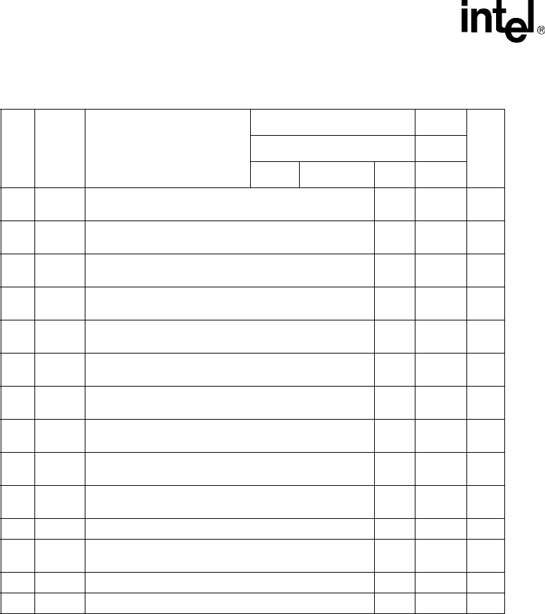
Table 20. Write Operations—64Mbit Density
#Sym Parameter
Density 64 Mbit
UnitProduct 80 ns
V
CC
2.7V–3.6V Note Min
W1
t
PHWL
/
t
PHEL
RP# High Recovery to WE# (CE#) Going Low 4,5 150 ns
W2
t
ELWL
/
t
WLEL
CE# (WE#) Setup to WE# (CE#) Going Low 4,5 0 ns
W3
t
WLWH
/
t
ELEH
WE#(CE#)PulseWidth 1,4,5 60 ns
W4
t
DVWH
/
t
DVEH
Data Setup to WE# (CE#) Going High 2,4,5 40 ns
W5
t
AVWH
/
t
AVEH
Address Setup to WE# (CE#) Going High 2,4,5 60 ns
W6
t
WHEH
/
t
EHWH
CE# (WE#) Hold Time from WE# (CE#) High 4,5 0 ns
W7
t
WHDX
/
t
EHDX
Data Hold Time from WE# (CE#) High 2,4,5 0 ns
W8
t
WHAX
/
t
EHAX
Address Hold Time from WE# (CE#) High 2,4,5 0 ns
W9
t
WHWL /
t
EHEL
WE#(CE#)PulseWidthHigh 1,4,5 30 ns
W10
t
VPWH
/
t
VPEH
V
PP
Setup to WE# (CE#) Going High 3,4,5 200 ns
W11 t
QVVL
V
PP
Hold from Valid SRD 3,4 0 ns
W12
t
BHWH
/
t
BHEH
WP#SetuptoWE#(CE#)GoingHigh 3,4 0 ns
W13 t
QVBL
WP# Hold from Valid SRD 3,4 0 ns
W14 t
WHGL
WE#HightoOE#GoingLow 3,4 30 ns
NOTES:
1. Write pulse width (t
WP
) is defined from CE# or WE# going low (whichever goes low last) to CE# or
WE# going high (whichever goes high first). Hence, t
WP
=t
WLWH
=t
ELEH
=t
WLEH
=t
ELWH
.
Similarly, write pulse width high (t
WPH
) is defined from CE# or WE# going high (whichever goes
high first) to CE# or WE# going low (whichever goes low last). Hence,
t
WPH
=t
WHWL
=t
EHEL
=t
WHEL
=t
EHWL
.
2. Refer to Table 7, “Command Bus Operations” on page 24 for valid A
IN
or D
IN
.
3. Sampled, but not 100% tested.
4. See Figure 11, “AC Input/Output Reference Waveform” on page 49 for timing measurements and
maximum allowable input slew rate.
5. See
Figure 9, “Write Operations Waveform” on page 47.
Intel
£
Advanced+ Boot Block Flash Memory (C3)
Datasheet 47
8.3 Erase and Program Timings
Table 21. Erase and Program Timings
Figure 9. Write Operations Waveform
Symbol Parameter
V
PP
1.65 V–3.6 V 11.4 V–12.6 V
Unit
Note Typ Max Typ Max
t
BWPB
4-KW Parameter Block
Word Program Time
1, 2, 3 0.10 0.30 0.03 0.12 s
t
BWMB
32-KW Main Block
Word Program Time
1, 2, 3 0.8 2.4 0.24 1 s
t
WHQV1
/t
EHQV1
Word Program Time for 0.13
and0.18MicronProduct
1, 2, 3 12 200 8 185 µs
Word Program Time for 0.25
Micron Product
1, 2, 3 22 200 8 185 µs
t
WHQV2
/t
EHQV2
4-KW Parameter Block
Erase Time
1, 2, 3 0.5 4 0.4 4 s
t
WHQV3
/t
EHQV3
32-KW Main Block
Erase Time
1, 2, 3 1 5 0.6 5 s
t
WHRH1
/t
EHRH1
Program Suspend Latency 1,3 5 10 5 10 µs
t
WHRH2
/t
EHRH2
Erase Suspend Latency 1,3 5 20 5 20 µs
NOTES:
1. Typical values measured at T
A
= +25 °C and nominal voltages.
2. Excludes external system-level overhead.
3. Sampled, but not 100% tested.
W10
W1
W7W4
W9W9
W3W3
W2
W6
W8W5
A
ddress [A]
CE# [E]
WE# [W]
OE# [G]
Data [D/Q]
RP# [P]
Vpp [V]
Intel
£
Advanced+ Boot Block Flash Memory (C3)
48 Datasheet
8.4 Reset Specifications
Table 22. Reset Specifications
Symbol Parameter Notes
V
CC
2.7V–3.6V
Unit
Min Max
t
PLPH
RP# Low to Reset during Read
(If RP# is tied to V
CC
, this specification is not
applicable)
1, 2 100 ns
t
PLRH1
RP# Low to Reset during Block Erase 3 22 µs
t
PLRH2
RP# Low to Reset during Program 3 12 µs
NOTES:
1. If t
PLPH
is < 100 ns the device may still reset but this is not guaranteed.
2. If RP# is asserted while a Block Erase or Word Program operation is not executing, the reset will complete
within 100 ns.
3. Sampled, but not 100% tested.
Figure 10. Reset Operations Waveforms
IH
V
IL
V
RP# (P)
PLPH
t
IH
V
IL
V
RP# (P)
PLPH
t
(A) Reset during Read Mode
Abort
Complete
PHQV
t
PHWL
t
PHEL
t
PHQV
t
PHWL
t
PHEL
t
(B) Reset during Program or Block Erase, <
PLPH
t
PLR
H
t
PLRH
t
IH
V
IL
V
RP# (P)
PLPH
t
Abort
Complete
PHQV
t
PHWL
t
PHEL
t
PLRH
t
Deep
Power-
Down
(C) Reset Program or Block Erase, >
PLPH
t
PLRH
t
PREVIOUS910111213141516171819202122NEXT