Freelance Electronics Components Distributor
Closed Dec 25th-26th
800-300-1968
We Stock Hard to Find Parts

TE28F800C3BA90

Part # TE28F800C3BA90
Description NOR, Flash 512K x 16 48PinTSSOP
Category IC
Availability In Stock
Qty 375
Qty Price
1 - 78 $0.87249
79 - 157 $0.69403
158 - 236 $0.65437
237 - 315 $0.60810
316 + $0.54200
Manufacturer Available Qty
INTEL
Date Code: 0015
  • Shipping Freelance Stock: 190
    Ships Immediately
INTEL
Date Code: 0309
  • Shipping Freelance Stock: 16
    Ships Immediately
INTEL
Date Code: 0013
  • Shipping Freelance Stock: 167
    Ships Immediately
INTEL
Date Code: 0312
  • Shipping Freelance Stock: 2
    Ships Immediately


Technical Document


DISCLAIMER: The information provided herein is solely for informational purposes. Customers must be aware of the suitability of this product for their application, and consider that variable factors such as Manufacturer, Product Category, Date Codes, Pictures and Descriptions may differ from available inventory.

Intel
£
Advanced+ Boot Block Flash Memory (C3)
40 Datasheet
Table 14. Read Operations—16 Mbit Density
#Sym
Para-
mete
r
Density 16 Mbit
Unit Notes
Product
70 ns 80 ns 90 ns 110 ns
V
CC
2.7 V–3.6 V 2.7 V–3.6 V 3.0 V–3.6 V 2.7 V–3.6 V 3.0 V–3.6V 2.7 V–3.6V
Min Max Min Max Min Max Min Max Min Max Min Max
R1 t
AVAV
Read Cycle Time
70 80 80 90 100 110
ns 3,4
R2
t
AVQ
V
Address to
Output Delay
70 80 80 90 100 110
ns 3,4
R3
t
ELQ
V
CE# to Output
Delay
70 80 80 90 100 110
ns 1,3,4
R4
t
GLQ
V
OE# to Output
Delay
20 20 30 30 30 30
ns 1,3,4
R5
t
PHQ
V
RP# to Output
Delay
150 150 150 150 150 150
ns 3,4
R6
t
ELQ
X
CE# to Output in
Low Z
000000
ns 2,3,4
R7
t
GLQ
X
OE# to Output in
Low Z
000000
ns 2,3,4
R8
t
EHQ
Z
CE# to Output in
High Z
20 20 20 20 20 20
ns 2,3,4
R9
t
GHQ
Z
OE# to Output in
High Z
20 20 20 20 20 20
ns 2,3,4
R10 t
OH
Output Hold from
Address, CE#, or
OE# Change,
Whichever
Occurs First
000000
ns 2,3,4
NOTES:
1.OE#maybedelayeduptot
ELQV
t
GLQV
after the falling edge of CE# without impact on t
ELQV
.
2. Sampled, but not 100% tested.
3. See Figure 8, “Read Operation Waveform” on page 42.
4. See Figure 11, “AC Input/Output Reference Waveform” on page 49 for timing measurements and maximum allowable input
slew rate.
Intel
£
Advanced+ Boot Block Flash Memory (C3)
Datasheet 41
Table 15. Read Operations—32 Mbit Density
#Sym
Para-
meter
Density 32 Mbit
Unit Notes
Product
70 ns 90 ns 100 ns 110 ns
V
CC
2.7 V–3.6 V 2.7 V–3.6 V 3.0 V–3.3 V 2.7 V–3.3 V 3.0 V–3.3 V 2.7 V–3.3 V
Min Max Min Max Min Max Min Max Min Max Min Max
R1 t
AVAV
Read Cycle Time
70 90 90 100 100 110
ns 3,4
R2
t
AVQ
V
Address to Output
Delay
70 90 90 100 100 110
ns 3,4
R3
t
ELQ
V
CE# to Output
Delay
70 90 90 100 100 110
ns 1,3,4
R4
t
GLQ
V
OE# to Output
Delay
20 20 30 30 30 30
ns 1,3,4
R5
t
PHQ
V
RP# to Output
Delay
150 150 150 150 150 150
ns 3,4
R6
t
ELQ
X
CE# to Output in
Low Z
000000
ns 2,3,4
R7
t
GLQ
X
OE# to Output in
Low Z
000000
ns 2,3,4
R8
t
EHQ
Z
CE# to Output in
High Z
20 20 20 20 20 20
ns 2,3,4
R9
t
GHQ
Z
OE# to Output in
High Z
20 20 20 20 20 20
ns 2,3,4
R10 t
OH
Output Hold from
Address, CE#, or
OE# Change,
Whichever
Occurs First
000000
ns 2,3,4
NOTES:
1.OE#maybedelayeduptot
ELQV
t
GLQV
after the falling edge of CE# without impact on t
ELQV
.
2. Sampled, but not 100% tested.
3. See Figure 8, “Read Operation Waveform” on page 42.
4. See Figure 11, “AC Input/Output Reference Waveform on page 49 for timing measurements and maximum allowable
input slew rate.
Intel
£
Advanced+ Boot Block Flash Memory (C3)
42 Datasheet
Table 16. Read Operations — 64 Mbit Density
#Sym Parameter
Density 64 Mbit
Unit
Product 70 ns 80 ns
V
CC
2.7 V–3.6 V 2.7 V–3.6 V
Note Min Max Min Max
R1 t
AVAV
Read Cycle Time 3,4 70 80 ns
R2 t
AVQV
Address to Output Delay 3,4 70 80 ns
R3 t
ELQV
CE# to Output Delay 1,3,4 70 80 ns
R4 t
GLQV
OE# to Output Delay 1,3,4 20 20 ns
R5 t
PHQV
RP# to Output Delay 3,4 150 150 ns
R6 t
ELQX
CE#toOutputinLowZ 2,3,4 0 0 ns
R7 t
GLQX
OE# to Output in Low Z 2,3,4 0 0 ns
R8 t
EHQZ
CE#toOutputinHighZ 2,3,4 20 20 ns
R9 t
GHQZ
OE# to Output in High Z 2,3,4 20 20 ns
R10 t
OH
Output Hold from Address, CE#, or OE#
Change, Whichever Occurs First
2,3,4 0 0 ns
NOTES:
1.OE#maybedelayeduptot
ELQV–
t
GLQV
after the falling edge of CE# without impact on t
ELQV
.
2. Sampled, but not 100% tested.
3. See Figure 8, Read Operation Waveform” on page 42.
4. See Figure 11, “AC Input/Output Reference Waveform” on page 49 for timing measurements and
maximum allowable input slew rate.
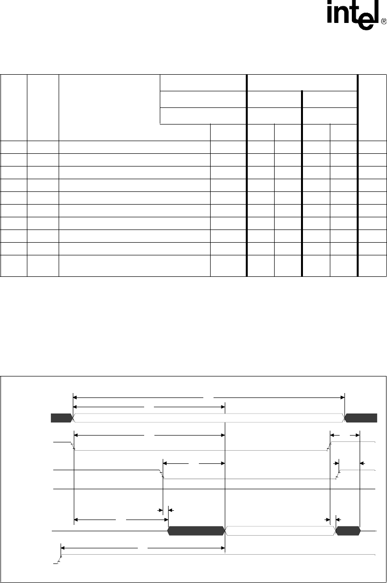
Figure 8. Read Operation Waveform
R5
R10
R7
R6
R9R4
R8R3
R1
R2
R1
A
ddress [A]
CE# [E]
OE# [G]
WE# [W]
Data [D/Q]
RST # [P]
PREVIOUS7891011121314151617181920NEXT