Closed Dec 25th-26th
800-300-1968
We Stock Hard to Find Parts
My Account
|
My Orders
|
My Cart
Questions?
(800) 300-1968
Register
(current)
My Account
(current)
My Orders
(current)
My Cart
(current)
Categories
(current)
Manufacturers
Request a Quote
Sell Your Excess
Consignment
Quality Assurance
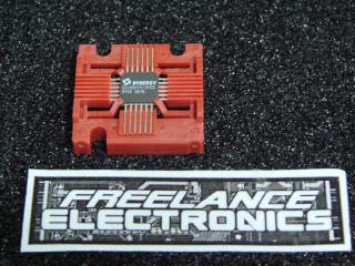
SY100S325JC
Part #
SY100S325JC
Description
IC TRANSLATOR HEX LP 28-PLCC
Category
IC
Availability
In Stock
Qty
26
Qty
Price
1 - 5
$11.15213
6 - 10
$8.87101
11 - 16
$8.36409
17 - 21
$7.77269
22 +
$6.92784
Manufacturer
Available
Qty
SYNERGY
Date Code: 0050
Freelance Stock:
1
Ships Immediately
SYNERGY
Date Code: 0012
Freelance Stock:
2
Ships Immediately
SYNERGY
Date Code: 9722
Freelance Stock:
23
Ships Immediately
Add to Cart
Related Items
SYNERGY
IC
SY1001E131JC
SYNERGY
IC
SY100474-5FCS
SYNERGY
IC
SY100E016JC
$9.97117
SYNERGY
IC
SY100E111JC
$9.05120
SYNERGY
IC
SY100E137JC
$15.23256
SYNERGY
IC
SY100E150JC
$8.38484