Electrical and Thermal Characteristics
MPC5200B Data Sheet, Rev. 1
Freescale Semiconductor 25
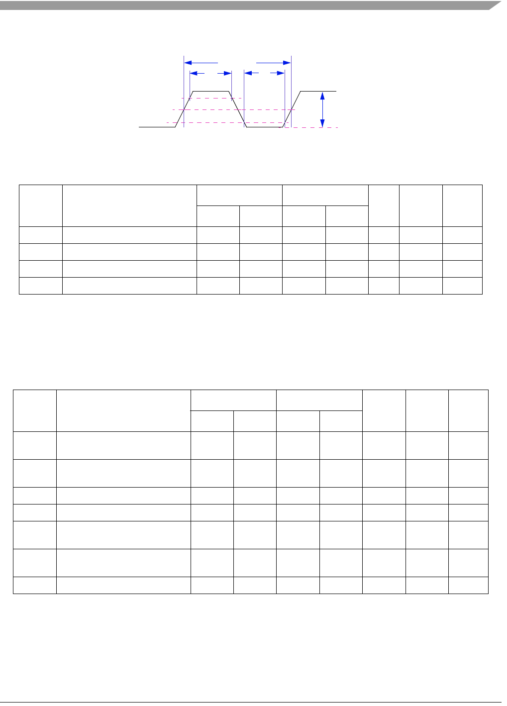
Figure 9. PCI CLK Waveform
NOTES:
1. In general, all 66-MHz PCI components must work with any clock frequency up to 66 MHz. CLK requirements vary
depending upon whether the clock frequency is above 33 MHz.
2. Rise and fall times are specified in terms of the edge rate measured in V/ns. This slew rate must be met across the minimum
peak-to-peak portion of the clock waveform as shown in Figure 9.
3. The minimum clock period must not be violated for any single clock cycle, i.e., accounting for all system jitter.
NOTES:
1. See the timing measurement conditions in the PCI Local Bus Specification [4]. It is important that all driven signal transitions
drive to their Voh or Vol level within one Tcyc.
2. Minimum times are measured at the package pin with the load circuit, and maximum times are measured with the load circuit
as shown in the PCI Local Bus Specification [4].
Table 22. PCI CLK Specifications
Sym Description
66 MHz 33 MHz
Units Notes SpecID
Min Max Min Max
t
cyc
PCI CLK Cycle Time 15 30 30 ns
(1),(3)
A6.1
t
high
PCI CLK High Time 6 11 ns A6.2
t
low
PCI CLK Low Time 6 11 ns A6.3
- PCI CLK Slew Rate 1.5 4 1 4 V/ns
(2)
A6.4
Table 23. PCI Timing Parameters
Sym Description
66 MHz 33 MHz
Units Notes SpecID
Min Max Min Max
t
val
CLK to Signal Valid Delay - bused
signals
26211ns
(1),(2),(3)
A6.5
t
val
(ptp) CLK to Signal Valid Delay - point
to point
26212ns
(1),(2),(3)
A6.6
t
on
Float to Active Delay 2 2 ns
(1)
A6.7
t
off
Active to Float Delay 14 28 ns
(1)
A6.8
t
su
Input Setup Time to CLK - bused
signals
37ns
(3),(4)
A6.9
t
su
(ptp) Input Setup Time to CLK - point
to point
5 10,12 ns
(3),(4)
A6.10
t
h
Input Hold Time from CLK 0 0 ns
(4)
A6.11
t
cyc
PCI CLK
t
low
t
high
0.4Vcc
0.4Vcc, p-to-p
0.3Vcc
0.5Vcc
0.6Vcc
0.2Vcc
(minimum)


