MPC5200B Data Sheet, Rev. 1
Electrical and Thermal Characteristics
Freescale Semiconductor24
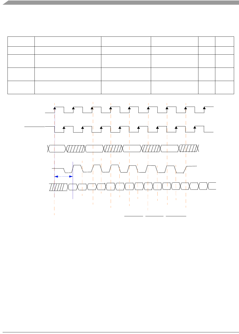
3.3.5.4 Memory Interface Timing-DDR SDRAM Write Command
Figure 8. DDR SDRAM Memory Write Timing
3.3.6 PCI
The PCI interface on the MPC5200B is designed to PCI Version 2.2 and supports 33-MHz and 66-MHz
PCI operations. See the PCI Local Bus Specification [4]; the component section specifies the electrical and
timing parameters for PCI components with the intent that components connect directly together whether
on the planar or an expansion board, without any external buffers or other “glue logic.” Parameters apply
at the package pins, not at expansion board edge connectors.
The MPC5200B is always the source of the PCI CLK. The clock waveform must be delivered to each
33-MHz or 66-MHz PCI component in the system. Figure 9 shows the clock waveform and required
measurement points for 3.3 V signaling environments. Table 22 summarizes the clock specifications.
Table 21. DDR SDRAM Memory Write Timing
Sym Description Min Max Units SpecID
t
mem_clk
MEM_CLK period 7.5 — ns A5.20
t
DQSS
Delay from write command to first
rising edge of MDQS
—t
mem_clk
+0.4 ns A5.21
data
valid
MDQ valid before rising edge of
MDQS
TBD ns A5.22
data
hold
MDQ valid after rising edge of
MDQS
TBD ns A5.23
MEM_CLK
Control Signals
MDQ (Data)
MEM_CLK
MDQS (Data Strobe)
NOTE: Control Signals signals are composed of RAS, CAS, MEM_WE
, MEM_CS, MEM_CS1 and CLK_EN
Write
WriteWrite
t
DQSS
Write


