Freelance Electronics Components Distributor
Closed Dec 25th-26th
800-300-1968
We Stock Hard to Find Parts

SPC5200CBV400B

Part # SPC5200CBV400B
Description MPU MPC52xx RISC 32-Bit 400MHz 2.5V/3.3V 272-Pin BGA Tray
Category IC
Availability Out of Stock
Qty 0
Qty Price
1 + $29.63318


Technical Document


DISCLAIMER: The information provided herein is solely for informational purposes. Customers must be aware of the suitability of this product for their application, and consider that variable factors such as Manufacturer, Product Category, Date Codes, Pictures and Descriptions may differ from available inventory.

Electrical and Thermal Characteristics
MPC5200B Data Sheet, Rev. 1
Freescale Semiconductor 19
NOTES:
1) The frequency of IP_CLK depends on register settings in Clock Distribution Module. See the MPC5200B User Manual [1].
2) The interrupt latency descriptions in the table above are related to non competitive, non masked but enabled external
interrupt sources. Take care of interrupt prioritization which may increase the latencies.
Since all external interrupt signals are synchronized into the internal processor bus clock domain, each of
these signals has to exceed a minimum pulse width of more than one IP_CLK cycle.
NOTES:
1) The frequency of the IP_CLK depends on the register settings in Clock Distribution Module. See the MPC5200B User
Manual [1] for further information.
2) If the same interrupt occurs a second time while its interrupt service routine has not cleared the former one, the second
interrupt will not be recognized at all.
Besides synchronization, prioritization, and mapping the latency of an external interrupt to the start of its
associated interrupt service routine also depends on the following conditions: To get a minimum interrupt
service response time, it is recommended to enable the instruction cache and set up the maximum core
clock, XL bus, and IP bus frequencies (depending on board design and programming). In addition, it is
advisable to execute an interrupt handler, which has been implemented in assembly code.
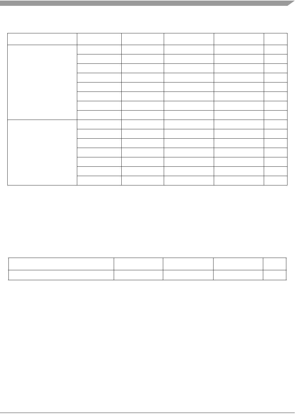
Standard GPIO Interrupts GPIO_PSC3_4 12 IP_CLK normal (int) A4.6
GPIO_PSC3_5 12 IP_CLK normal (int) A4.7
GPIO_PSC3_8 12 IP_CLK normal (int) A4.8
GPIO_USB_9 12 IP_CLK normal (int) A4.9
GPIO_ETHI_4 12 IP_CLK normal (int) A4.10
GPIO_ETHI_5 12 IP_CLK normal (int) A4.11
GPIO_ETHI_6 12 IP_CLK normal (int) A4.12
GPIO_
ETHI_7
12 IP_CLK normal (int) A4.13
GPIO WakeUp Interrupts GPIO_
PSC1_4
12 IP_CLK normal (int) A4.15
GPIO_PSC2_4 12 IP_CLK normal (int) A4.16
GPIO_PSC3_9 12 IP_CLK normal (int) A4.17
GPIO_ETHI_8 12 IP_CLK normal (int) A4.18
GPIO_IRDA_0 12 IP_CLK normal (int) A4.19
DGP_IN0 12 IP_CLK normal (int) A4.20
DGP_IN1 12 IP_CLK normal (int) A4.21
Table 17. Minimum Pulse Width for External Interrupts to be Recognized
Name Min Pulse Width Max Pulse Width Reference Clock SpecID
All external interrupts (IRQs, GPIOs) > 1 clock cycle IP_CLK A4.22
Table 16. External Interrupt Latencies (continued)
Interrupt Type Pin Name Clock Cycles Reference Clock Core Interrupt SpecID
MPC5200B Data Sheet, Rev. 1
Electrical and Thermal Characteristics
Freescale Semiconductor20
3.3.5 SDRAM
3.3.5.1 Memory Interface Timing-Standard SDRAM Read Command
Figure 5. Timing Diagram—Standard SDRAM Memory Read Timing
3.3.5.2 Memory Interface Timing-Standard SDRAM Write Command
In Standard SDRAM, all signals are activated on the MEM_CLK from the Memory Controller and
captured on the MEM_CLK clock at the memory device.
Table 18. Standard SDRAM Memory Read Timing
Sym Description Min Max Units SpecID
t
mem_clk
MEM_CLK period 7.5 ns A5.1
t
valid
Control Signals, Address and MBA Valid after
rising edge of MEM_CLK
—t
mem_clk
*0.5+0.4 ns A5.2
t
hold
Control Signals, Address and MBA Hold after
rising edge of MEM_CLK
t
mem_clk
*0.5 ns A5.3
DM
valid
DQM valid after rising edge of MEM_CLK t
mem_clk
*0.25+0.4 ns A5.4
DM
hold
DQM hold after rising edge of MEM_CLK t
mem_clk
*0.25-0.7 ns A5.5
data
setup
MDQ setup to rising edge of MEM_CLK 0.3 ns A5.6
data
hold
MDQ hold after rising edge of MEM_CLK 0.2 ns A5.7
MEM_CLK
Control Signals
MDQ (Data)
MA (Address)
NOTE: Control Signals are composed of RAS, CAS, MEM_WE
, MEM_CS, MEM_CS1 and CLK_EN
Active NOP READ NOPNOPNOP NOP
t
hold
Row Column
MBA (Bank Selects)
t
valid
t
hold
t
valid
t
hold
t
valid
DQM (Data Mask)
DM
valid
DM
hold
NOP
data
hold
data
setup
Electrical and Thermal Characteristics
MPC5200B Data Sheet, Rev. 1
Freescale Semiconductor 21
Figure 6. Timing Diagram—Standard SDRAM Memory Write Timing
3.3.5.3 Memory Interface Timing-DDR SDRAM Read Command
The SDRAM Memory Controller uses a 1/4 period delayed MDQS strobe to capture the MDQ data. The
1/4 period delay value is calculated automatically by hardware.
Table 19. Standard SDRAM Write Timing
Sym Description Min Max Units SpecID
t
mem_clk
MEM_CLK period 7.5 ns A5.8
t
valid
Control Signals, Address and MBA Valid
after rising edge of MEM_CLK
—t
mem_clk
*0.5+0.4 ns A5.9
t
hold
Control Signals, Address and MBA Hold after
rising edge of MEM_CLK
t
mem_clk
*0.5 ns A5.10
DM
valid
DQM valid after rising edge of MEM_CLK t
mem_clk
*0.25+0.4 ns A5.11
DM
hold
DQM hold after rising edge of Mem_clk t
mem_clk
*0.25-0.7 ns A5.12
data
valid
MDQ valid after rising edge of MEM_CLK t
mem_clk
*0.75+0.4 ns A5.13
data
hold
MDQ hold after rising edge of MEM_CLK t
mem_clk
*0.75-0.7 ns A5.14
MEM_CLK
Control Signals
MDQ (Data)
MA (Address)
NOTE: Control Signals are composed of RAS, CAS, MEM_WE
, MEM_CS, MEM_CS1 and CLK_EN
Active NOP WRITE NOPNOPNOPNOP NOP
t
hold
Row Column
MBA (Bank Selects)
data
hold
data
valid
t
valid
t
hold
t
valid
t
hold
t
valid
DQM (Data Mask)
DM
valid
DM
hold
PREVIOUS12345678910111213NEXT