Freelance Electronics Components Distributor
Closed Dec 25th-26th
800-300-1968
We Stock Hard to Find Parts

SPC5200CBV400B

Part # SPC5200CBV400B
Description MPU MPC52xx RISC 32-Bit 400MHz 2.5V/3.3V 272-Pin BGA Tray
Category IC
Availability Out of Stock
Qty 0
Qty Price
1 + $29.63318


Technical Document


DISCLAIMER: The information provided herein is solely for informational purposes. Customers must be aware of the suitability of this product for their application, and consider that variable factors such as Manufacturer, Product Category, Date Codes, Pictures and Descriptions may differ from available inventory.

Package Description
MPC5200B Data Sheet, Rev. 1
Freescale Semiconductor 67
TIMER_1 I/O VDD_IO DRV4 TTL
TIMER_2 MOSI I/O VDD_IO DRV4 TTL
TIMER_3 MISO I/O VDD_IO DRV4 TTL
TIMER_4 SS I/O VDD_IO DRV4 TTL
TIMER_5 SCK I/O VDD_IO DRV4 TTL
TIMER_6 I/O VDD_IO DRV4 TTL
TIMER_7 I/O VDD_IO DRV4 TTL
Clock
SYS_XTAL_IN Input VDD_IO
SYS_XTAL_OUT Output VDD_IO
RTC_XTAL_IN Input VDD_IO
RTC_XTAL_OUT Output VDD_IO
Misc
PORRESET
Input VDD_IO DRV4 Schmitt
HRESET
I/O VDD_IO DRV8_OD
1
Schmitt
SRESET
I/O VDD_IO DRV8_OD
1
Schmitt
IRQ0 I/O VDD_IO DRV4 TTL
IRQ1 I/O VDD_IO DRV4 TTL
IRQ2 I/O VDD_IO DRV4 TTL
IRQ3 I/O VDD_IO DRV4 TTL
Test/Configuration
SYS_PLL_TPA I/O VDD_IO DRV4 TTL
TEST_MODE_0 Input VDD_IO DRV4 TTL
TEST_MODE_1 Input VDD_IO DRV4 TTL
TEST_SEL_0 I/O VDD_IO DRV4 TTL PULLUP
TEST_SEL_1 I/O VDD_IO DRV8 TTL
JTAG_TCK TCK Input VDD_IO DRV4 Schmitt PULLUP
JTAG_TDI TDI Input VDD_IO DRV4 TTL PULLUP
JTAG_TDO TDO I/O VDD_IO DRV8 TTL
JTAG_TMS TMS Input VDD_IO DRV4 TTL PULLUP
JTAG_TRST
TRST Input VDD_IO DRV4 TTL PULLUP
Power and Ground
VDD_IO -
Table 52. MPC5200B Pinout Listing (continued)
Name Alias Type Power Supply
Output Driver
Type
Input
Type
Pull-up/
down
MPC5200B Data Sheet, Rev. 1
System Design Information
Freescale Semiconductor68
5 System Design Information
5.1 Power Up/Down Sequencing
Figure 51 shows situations in sequencing the I/O VDD (VDD_IO), Memory VDD (VDD_IO_MEM), PLL
VDD (PLL_AVDD), and Core VDD (VDD_CORE).
VDD_MEM_IO -
VDD_CORE -
VSS_IO/CORE -
SYS_PLL_AVDD -
CORE_PLL_AVDD -
NOTES:
1
All “open drain” outputs of the MPC5200B are actually regular three-state output drivers with the output data tied
low and the output enable controlled. Thus, unlike a true open drain, there is a current path from the external
system to the MPC5200B I/O power rail if the external signal is driven above the MPC5200B I/O power rail voltage.
Table 52. MPC5200B Pinout Listing (continued)
Name Alias Type Power Supply
Output Driver
Type
Input
Type
Pull-up/
down
System Design Information
MPC5200B Data Sheet, Rev. 1
Freescale Semiconductor 69
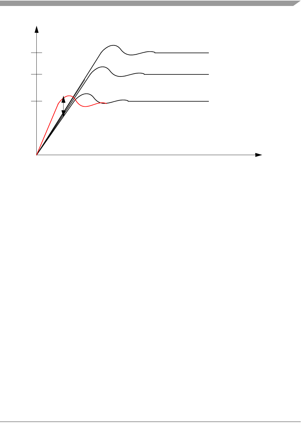
Figure 51. Supply Voltage Sequencing
The relationship between VDD_IO_MEM and VDD_IO is non-critical during power-up and power-down
sequences. Both VDD_IO_MEM (2.5 V or 3.3 V) and VDD_IO are specified relative to VDD_CORE.
5.1.1 Power Up Sequence
If VDD_IO/VDD_IO_MEM are powered up with the VDD_CORE at 0V, the sense circuits in the I/O pads
will cause all pad output drivers connected to the VDD_IO/VDD_IO_MEM to be in a high-impedance
state. There is no limit to how long after VDD_IO/VDD_IO_MEM powers up before VDD_CORE must
power up. VDD_CORE should not lead the VDD_IO, VDD_IO_MEM or PLL_AVDD by more than 0.4
V during power ramp up or there will be high current in the internal ESD protection diodes. The rise times
on the power supplies should be slower than 1 microsecond to avoid turning on the internal ESD protection
clamp diodes.
The recommended power up sequence is as follows:
Use one microsecond or slower rise time for all supplies.
VDD_CORE/PLL_AVDD and VDD_IO/VDD_IO_MEM should track up to 0.9 V and then separate for
the completion of ramps with VDD_IO/VDD_IO_MEM going to the higher external voltages. One way
to accomplish this is to use a low drop-out voltage regulator.
1.5V
2.5V
3.3V
0
DC Power Supply Voltage
VDD_IO,
VDD_IO_MEM (SDR)
VDD_IO_MEM (DDR)
VDD_CORE,
PLL_AVDD
Note:
1. VDD_CORE should not exceed VDD_IO, VDD_IO_MEM or PLL_AVDD by more
than 0.4 V at any time, including power-up.
2. It is recommended that VDD_CORE/PLL_AVDD should track
VDD_IO/VDD_IO_MEM up to 0.9 V then separate for completion of ramps.
3. Input voltage must not be greater than the supply voltage (VDD_IO)
VDD_IO_MEM, VDD_CORE, or PLL_AVDD) by more than 0.5 V at any time,
1
2
Time
PREVIOUS1617181920212223242526NEXT