Electrical and Thermal Characteristics
MPC5200B Data Sheet, Rev. 1
Freescale Semiconductor 59
3.3.17 IEEE 1149.1 (JTAG) AC Specifications
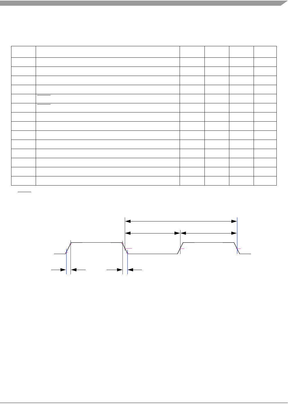
Figure 46. Timing Diagram—JTAG Clock Input
Table 51. JTAG Timing Specification
Sym Characteristic Min Max Unit SpecID
— TCK frequency of operation. 0 25 MHz A17.1
1 TCK cycle time. 40 — ns A17.2
2 TCK clock pulse width measured at 1.5V. 1.08 — ns A17.3
3 TCK rise and fall times. 0 3 ns A17.4
4TRST
setup time to tck falling edge
(1)
.
NOTES:
1
TRST is an asynchronous signal. The setup time is for test purposes only.
10 — ns A17.5
5TRST
assert time. 5 — ns A17.6
6 Input data setup time
(2)
.
2
Non-test, other than TDI and TMS, signal input timing with respect to TCK.
5 — ns A17.7
7 Input data hold time
(2)
. 15 — ns A17.8
8 TCK to output data valid
(3)
.
3
Non-test, other than TDO, signal output timing with respect to TCK.
030nsA17.9
9 TCK to output high impedance
(3)
. 0 30 ns A17.10
10 TMS, TDI data setup time. 5 — ns A17.11
11 TMS, TDI data hold time. 1 — ns A17.12
12 TCK to TDO data valid. 0 15 ns A17.13
13 TCK to TDO high impedance. 0 15 ns A17.14
TCK
VMVM VM
3
3
22
1
VM = Midpoint Voltage
Numbers shown reference Table 51.


