Freelance Electronics Components Distributor
Closed Dec 25th-26th
800-300-1968
We Stock Hard to Find Parts

SPC5200CBV400B

Part # SPC5200CBV400B
Description MPU MPC52xx RISC 32-Bit 400MHz 2.5V/3.3V 272-Pin BGA Tray
Category IC
Availability Out of Stock
Qty 0
Qty Price
1 + $29.63318


Technical Document


DISCLAIMER: The information provided herein is solely for informational purposes. Customers must be aware of the suitability of this product for their application, and consider that variable factors such as Manufacturer, Product Category, Date Codes, Pictures and Descriptions may differ from available inventory.

MPC5200B Data Sheet, Rev. 1
Electrical and Thermal Characteristics
Freescale Semiconductor52
Figure 38. Timing Diagram — 8,16, 24, and 32-bit CODEC / I
2
S Slave Mode
3.3.15.2 AC97 Mode
NOTE
Output timing is specified at a nominal 50 pF load.
Table 44. Timing Specifications — AC97 Mode
Sym Description Min Typ Max Units SpecID
1 Bit Clock cycle time 81.4 ns A15.15
2 Clock pulse high time 40.7 ns A15.16
3 Clock pulse low time 40.7 ns A15.17
4 FrameSync valid after rising clock edge 13.0 ns A15.18
5 Output Data valid after rising clock edge 14.0 ns A15.19
6 Input Data setup time 1.0 ns A15.20
7 Input Data hold time 1.0 ns A15.21
BitClk
3
(CLKPOL=0)
BitClk
(CLKPOL=1)
FrameSync
(SyncPol = 1)
TxD
Output
Input
Input
4
5
Input
FrameSync
(SyncPol = 0)
Input
RxD
Input
1
22
6
Electrical and Thermal Characteristics
MPC5200B Data Sheet, Rev. 1
Freescale Semiconductor 53
Figure 39. Timing Diagram — AC97 Mode
3.3.15.3 IrDA Mode
NOTE
Output timing is specified at a nominal 50 pF load.
Figure 40. Timing Diagram — IrDA Transmit Line
Table 45. Timing Specifications — IrDA Transmit Line
Sym Description Min Max Units SpecID
1 Pulse high time, defined in the IrDA protocol definition 0.125 10000 µs A15.22
2 Pulse low time, defined in the IrDA protocol definition 0.125 10000 µs A15.23
3 Transmitter rising time 7.9 ns A15.24
4 Transmitter falling time 7.9 ns A15.25
BitClk
(CLKPOL=0)
FrameSync
(SyncPol = 1)
Sdata_out
Output
Input
6
Output
Sdata_in
Input
1
4
3
5
2
7
IrDA_TX
4
3
(SIR / FIR / MIR)
12
MPC5200B Data Sheet, Rev. 1
Electrical and Thermal Characteristics
Freescale Semiconductor54
3.3.15.4 SPI Mode
NOTE
Output timing is specified at a nominal 50 pF load.
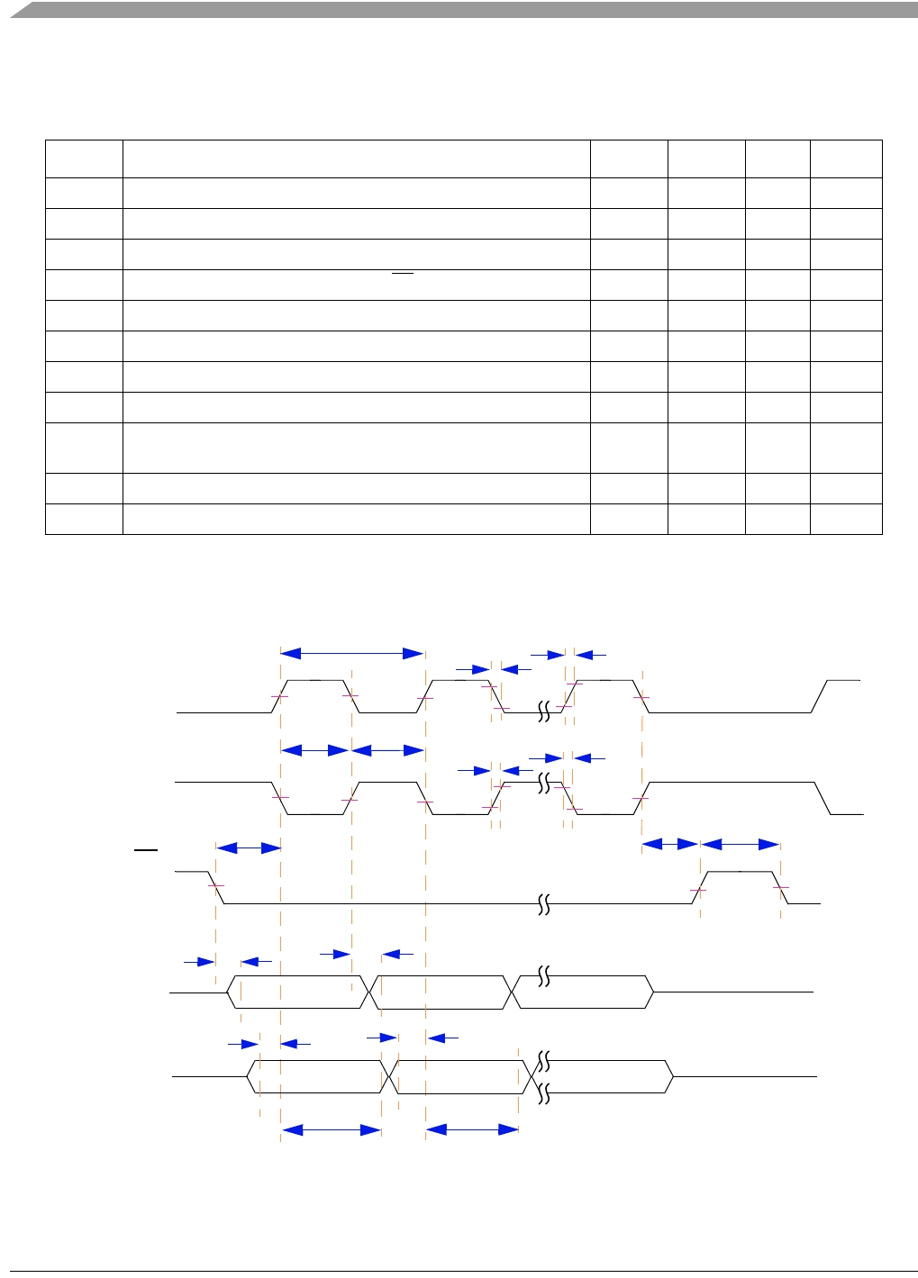
Figure 41. Timing Diagram — SPI Master Mode, Format 0 (CPHA = 0)
Table 46. Timing Specifications — SPI Master Mode, Format 0 (CPHA = 0)
Sym Description Min Max Units SpecID
1 SCK cycle time, programable in the PSC CCS register 30.0 ns A15.26
2 SCK pulse width, 50% SCK duty cycle 15.0 ns A15.27
3 Slave select clock delay, programable in the PSC CCS register 30.0 ns A15.28
4 Output Data valid after Slave Select (SS) 8.9 ns A15.29
5 Output Data valid after SCK 8.9 ns A15.30
6 Input Data setup time 6.0 ns A15.31
7 Input Data hold time 1.0 ns A15.32
8 Slave disable lag time 8.9 ns A15.33
9 Sequential Transfer delay, programable in the PSC CTUR / CTLR
register
15.0 ns A15.34
10 Clock falling time 7.9 ns A15.35
11 Clock rising time 7.9 ns A15.36
SCK
(CLKPOL=0)
SCK
(CLKPOL=1)
MOSI
Output
Output
Output
SS
Output
MISO
Input
1
22
8
9
3
4
5
6
6
7
7
11
10
10
11
PREVIOUS1112131415161718192021222324NEXT