Electrical and Thermal Characteristics
MPC5200B Data Sheet, Rev. 1
Freescale Semiconductor 49
3.3.13 I
2
C
NOTE
Output timing is specified at a nominal 50 pF load.
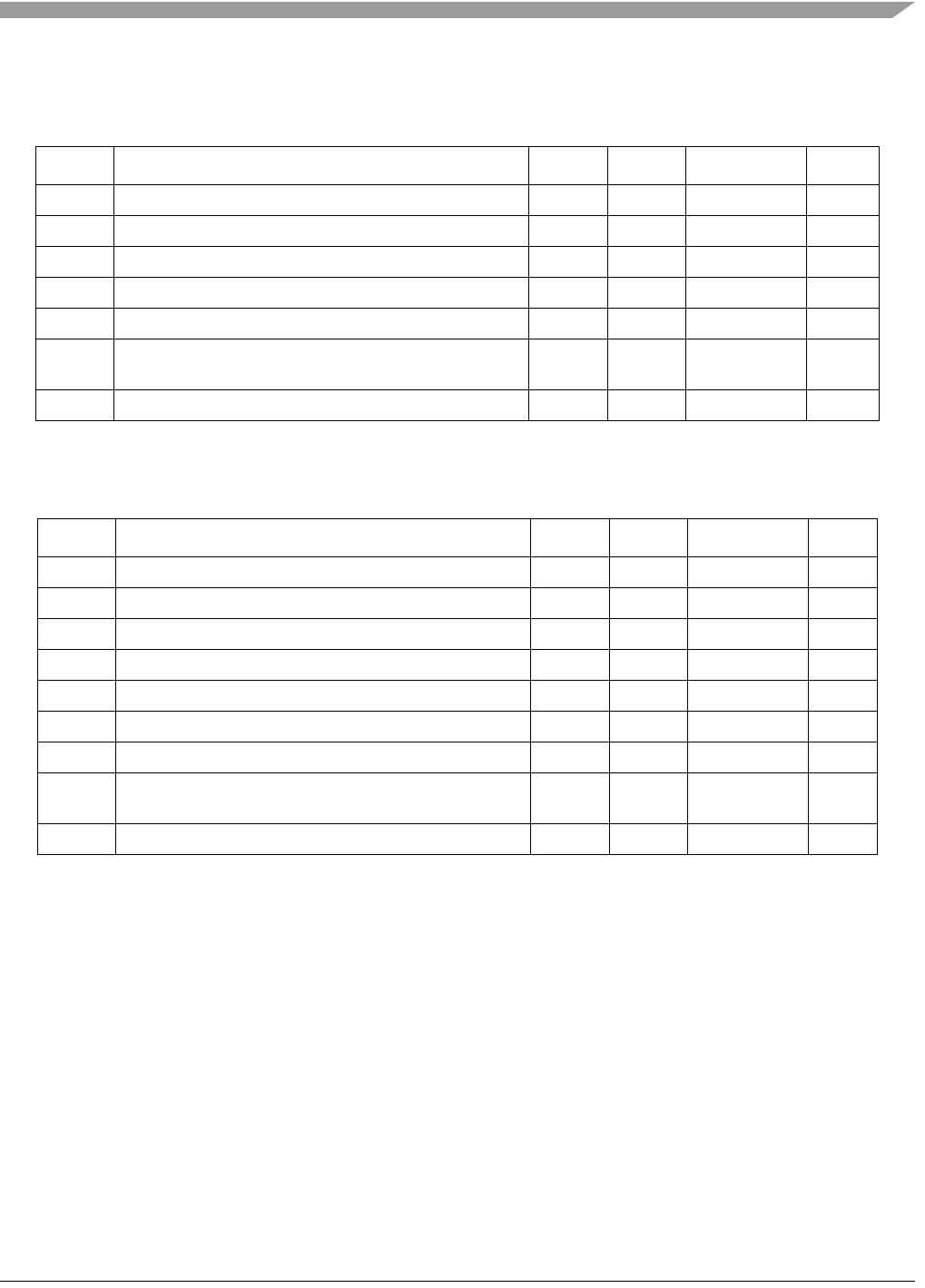
Table 40. I
2
C Input Timing Specifications—SCL and SDA
Sym Description Min Max Units SpecID
1 Start condition hold time 2 — IP-Bus Cycle
(1)
NOTES:
1
Inter Peripheral Clock is defined in the MPC5200B User Manual [1].
A13.1
2 Clock low time 8 — IP-Bus Cycle
(1)
A13.2
4 Data hold time 0.0 — ns A13.3
6 Clock high time 4 — IP-Bus Cycle
(1)
A13.4
7 Data setup time 0.0 — ns A13.5
8 Start condition setup time (for repeated start condition
only)
2 — IP-Bus Cycle
(1)
A13.6
9 Stop condition setup time 2 — IP-Bus Cycle
(1)
A13.7
Table 41. I
2
C Output Timing Specifications—SCL and SDA
Sym Description Min Max Units SpecID
1
(1)
NOTES:
1
Programming IFDR with the maximum frequency (IFDR=0x20) results in the minimum output timings listed. The
I
2
C interface is designed to scale the data transition time, moving it to the middle of the SCL low period. The actual
position is affected by the prescale and division values programmed in IFDR.
Start condition hold time 6 — IP-Bus Cycle
(3)
A13.8
2
(1)
Clock low time 10 — IP-Bus Cycle
(3)
A13.9
3
(2)
2
Because SCL and SDA are open-drain-type outputs, which the processor can only actively drive low, the time SCL
or SDA takes to reach a high level depends on external signal capacitance and pull-up resistor values
SCL/SDA rise time — 7.9 ns A13.10
4
(1)
Data hold time 7 — IP-Bus Cycle
(3)
A13.11
5
(1)
SCL/SDA fall time — 7.9 ns A13.12
6
(1)
Clock high time 10 — IP-Bus Cycle
(3)
A13.13
7
(1)
Data setup time 2 — IP-Bus Cycle
(3)
A13.14
8
(1)
Start condition setup time (for repeated start condition
only)
20 — IP-Bus Cycle
(3)
A13.15
9
(1)
Stop condition setup time 10 — IP-Bus Cycle
(3)
3
Inter Peripheral Clock is defined in the MPC5200B User Manual [1].
A13.16


