Freelance Electronics Components Distributor
Closed Dec 25th-26th
800-300-1968
We Stock Hard to Find Parts

SPC5200CBV400B

Part # SPC5200CBV400B
Description MPU MPC52xx RISC 32-Bit 400MHz 2.5V/3.3V 272-Pin BGA Tray
Category IC
Availability Out of Stock
Qty 0
Qty Price
1 + $29.63318


Technical Document


DISCLAIMER: The information provided herein is solely for informational purposes. Customers must be aware of the suitability of this product for their application, and consider that variable factors such as Manufacturer, Product Category, Date Codes, Pictures and Descriptions may differ from available inventory.

MPC5200B Data Sheet, Rev. 1
Electrical and Thermal Characteristics
Freescale Semiconductor46
NOTE
Output timing is specified at a nominal 50 pF load.
Figure 33. Timing Diagram — SPI Slave Mode, Format 0 (CPHA = 0)
Table 37. Timing Specifications — SPI Slave Mode, Format 0 (CPHA = 0)
Sym Description Min Max Units SpecID
1 Cycle time 4 1024 IP-Bus Cycle
(1)
NOTES:
1
Inter Peripheral Clock is defined in the MPC5200B User Manual [1].
A11.12
2 Clock high or low time 2 512 IP-Bus Cycle
(1)
A11.13
3 Slave select to clock delay 15.0 ns A11.14
4 Output Data valid after Slave Select (SS) 50.0 ns A11.15
5 Output Data valid after SCK 50.0 ns A11.16
6 Input Data setup time 50.0 ns A11.17
7 Input Data hold time 0.0 ns A11.18
8 Slave disable lag time 15.0 ns A11.19
9 Sequential Transfer delay 1 IP-Bus Cycle
(1)
A11.20
SCK
(CLKPOL=0)
SCK
(CLKPOL=1)
MOSI
Input
Input
Input
SS
Input
MISO
Output
1
22
9
3
7
4
6
5
8
Electrical and Thermal Characteristics
MPC5200B Data Sheet, Rev. 1
Freescale Semiconductor 47
NOTE
Output timing is specified at a nominal 50 pF load.
Figure 34. Timing Diagram — SPI Master Mode, Format 1 (CPHA = 1)
Table 38. Timing Specifications — SPI Master Mode, Format 1 (CPHA = 1)
Sym Description Min Max Units SpecID
1 Cycle time 4 1024 IP-Bus Cycle
(1)
NOTES:
1
Inter Peripheral Clock is defined in the MPC5200B User Manual [1].
A11.21
2 Clock high or low time 2 512 IP-Bus Cycle
(1)
A11.22
3 Slave select to clock delay 15.0 ns A11.23
4 Output data valid 20.0 ns A11.24
5 Input Data setup time 20.0 ns A11.25
6 Input Data hold time 20.0 ns A11.26
7 Slave disable lag time 15.0 ns A11.27
8 Sequential Transfer delay 1 IP-Bus Cycle
(1)
A11.28
9 Clock falling time 7.9 ns A11.29
10 Clock rising time 7.9 ns A11.30
SCK
(CLKPOL=0)
SCK
(CLKPOL=1)
MOSI
Output
Output
Output
SS
Output
MISO
Input
1
22
7
8
3
4
6
10
9
9
10
5
MPC5200B Data Sheet, Rev. 1
Electrical and Thermal Characteristics
Freescale Semiconductor48
NOTE
Output timing is specified at a nominal 50 pF load.
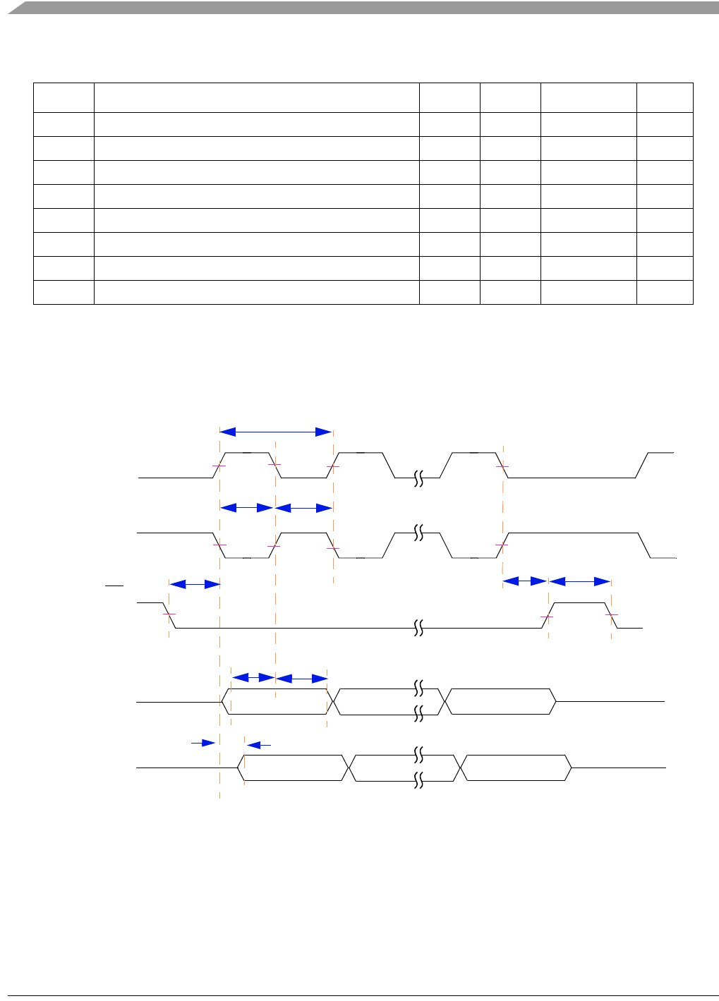
Figure 35. Timing Diagram — SPI Slave Mode, Format 1 (CPHA = 1)
3.3.12 MSCAN
The CAN functions are available as RX and TX pins at normal IO pads (I
2
C1+GPTimer or PSC2). There
is no filter for the WakeUp dominant pulse. Any High-to-Low edge can cause WakeUp, if configured.
Table 39. Timing Specifications — SPI Slave Mode, Format 1 (CPHA = 1)
Sym Description Min Max Units SpecID
1 Cycle time 4 1024 IP-Bus Cycle
(1)
NOTES:
1
Inter Peripheral Clock is defined in the MPC5200B User Manual [1].
A11.31
2 Clock high or low time 2 512 IP-Bus Cycle
(1)
A11.32
3 Slave select to clock delay 15.0 ns A11.33
4 Output data valid 50.0 ns A11.34
5 Input Data setup time 50.0 ns A11.35
6 Input Data hold time 0.0 ns A11.36
7 Slave disable lag time 15.0 ns A11.37
8 Sequential Transfer delay 1 IP-Bus Cycle
(1)
A11.38
SCK
(CLKPOL=0)
SCK
(CLKPOL=1)
MOSI
Input
Input
Input
SS
Input
MISO
Output
1
22
7
8
3
4
6
5
PREVIOUS910111213141516171819202122NEXT