Freelance Electronics Components Distributor
Closed Dec 25th-26th
800-300-1968
We Stock Hard to Find Parts

SPC5200CBV400B

Part # SPC5200CBV400B
Description MPU MPC52xx RISC 32-Bit 400MHz 2.5V/3.3V 272-Pin BGA Tray
Category IC
Availability Out of Stock
Qty 0
Qty Price
1 + $29.63318


Technical Document


DISCLAIMER: The information provided herein is solely for informational purposes. Customers must be aware of the suitability of this product for their application, and consider that variable factors such as Manufacturer, Product Category, Date Codes, Pictures and Descriptions may differ from available inventory.

Electrical and Thermal Characteristics
MPC5200B Data Sheet, Rev. 1
Freescale Semiconductor 43
Figure 29. Ethernet Timing Diagram—MII Async
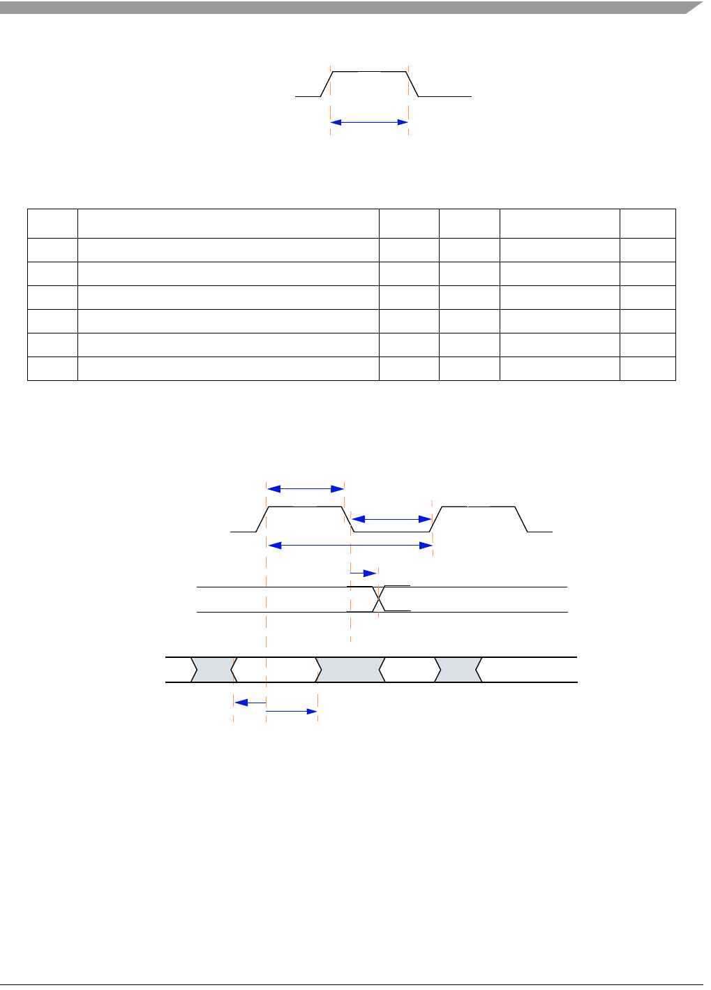
Figure 30. Ethernet Timing Diagram—MII Serial Management
Table 34. MII Serial Management Channel Signal Timing
Sym Description Min Max Unit SpecID
t
10
MDC falling edge to MDIO output delay 0 25 ns A9.10
t
11
MDIO (input) to MDC rising edge setup 10 ns A9.11
t
12
MDIO (input) to MDC rising edge hold 10 ns A9.12
t
13
MDC pulse width high
(1)
NOTES:
1
MDC is generated by MPC5200B with a duty cycle of 50% except when MII_SPEED in the FEC MII_SPEED
control register is changed during operation. See the MPC5200B User Manual [1].
160 ns A9.13
t
14
MDC pulse width low
(1)
160 ns A9.14
t
15
MDC period
(2)
2
The MDC period must be set to a value of less than or equal to 2.5 MHz (to be compliant with the IEEE MII
characteristic) by programming the FEC MII_SPEED control register. See the MPC5200B User Manual [1].
400 ns A9.15
t
9
CRS, COL
t
14
t
13
t
12
MDC (Output)
MDIO (Input)
MDIO (Output)
t
11
t
10
t
15
MPC5200B Data Sheet, Rev. 1
Electrical and Thermal Characteristics
Freescale Semiconductor44
3.3.10 USB
NOTE
Output timing is specified at a nominal 50 pF load.
Figure 31. Timing Diagram—USB Output Line
Table 35. Timing Specifications—USB Output Line
Sym Description Min Max Units SpecID
1 USB Bit width
(1)
NOTES:
1
Defined in the USB config register, (12 Mbit/s or 1.5 Mbit/s mode).
83.3 667 ns A10.1
2 Transceiver enable time 83.3 667 ns A10.2
3 Signal falling time 7.9 ns A10.3
4 Signal rising time 7.9 ns A10.4
11
2
4
3
3
4
USB_OE
USB_TXN
USB_TXP
Electrical and Thermal Characteristics
MPC5200B Data Sheet, Rev. 1
Freescale Semiconductor 45
3.3.11 SPI
NOTE
Output timing is specified at a nominal 50 pF load.
Figure 32. Timing Diagram — SPI Master Mode, Format 0 (CPHA = 0)
Table 36. Timing Specifications — SPI Master Mode, Format 0 (CPHA = 0)
Sym Description Min Max Units SpecID
1
Cycle time
4 1024 IP-Bus Cycle
(1)
NOTES:
1
Inter Peripheral Clock is defined in the MPC5200B User Manual [1].
A11.1
2
Clock high or low time
2 512 IP-Bus Cycle
(1)
A11.2
3
Slave select to clock delay
15.0 ns A11.3
4
Output Data valid after Slave Select (SS)
20.0 ns A11.4
5
Output Data valid after SCK
20.0 ns A11.5
6
Input Data setup time
20.0 ns A11.6
7
Input Data hold time
20.0 ns A11.7
8
Slave disable lag time
15.0 ns A11.8
9
Sequential transfer delay
1 IP-Bus Cycle
(1)
A11.9
10
Clock falling time
7.9 ns A11.10
11
Clock rising time
7.9 ns A11.11
SCK
(CLKPOL=0)
SCK
(CLKPOL=1)
MOSI
Output
Output
Output
SS
Output
MISO
Input
1
22
8
9
3
4
5
6
6
7
7
11
10
10
11
PREVIOUS89101112131415161718192021NEXT