Electrical and Thermal Characteristics
MPC5200B Data Sheet, Rev. 1
Freescale Semiconductor 35
NOTES:
1 t
UI
, t
MLI
, t
LI
indicate sender-to-recipient or recipient-to-sender interlocks. That is, one agent (either sender or recipient) is
waiting for the other agent to respond with a signal before proceeding.
•t
UI
is an unlimited interlock that has no maximum time value.
•t
MLI
is a limited time-out that has a defined minimum.
•t
LI
is a limited time-out that has a defined maximum.
2 All timing parameters are measured at the connector of the drive to which the parameter applies. For example, the sender
shall stop generating STROBE edges t
RFS
after negation of DMARDY. Both STROBE and DMARDY timing measurements
are taken at the connector of the sender. Even though the sender stops generating STROBE edges, the receiver may receive
additional STROBE edges due to propagation delays. All timing measurement switching points (low to high and high to low)
are taken at 1.5 V.
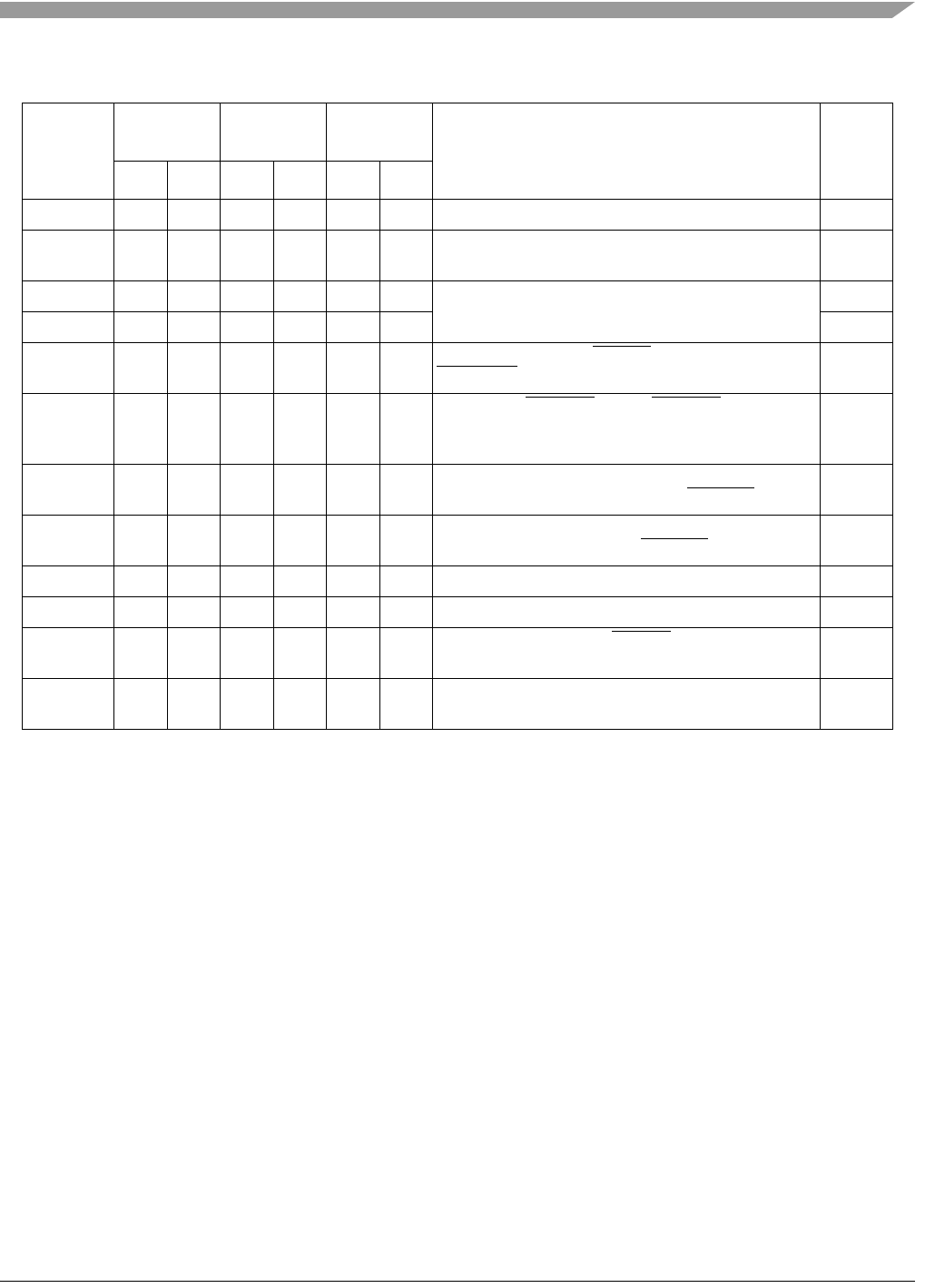
t
UI
0 — 0 — 0 — Unlimited interlock time.
A8.35
t
AZ
— 10 — 10 — 10 Maximum time allowed for output drivers to release
from being asserted or negated
A8.36
t
ZAH
20 — 20 — 20 — Minimum delay time required for output drivers to
assert or negate from released state
A8.37
t
ZAD
0—0—0— A8.38
t
ENV
20 70 20 70 20 70 Envelope time—from DMACK to STOP and
HDMARDY
during data out burst initiation.
A8.39
t
SR
— 50 — 30 — 20 STROBE to DMARDY time, if DMARDY is negated
before this long after STROBE edge, the recipient
receives no more than one additional data word.
A8.40
t
RFS
— 75 — 60 — 50 Ready-to-Final STROBE time—no STROBE edges
are sent this long after negation of DMARDY.
A8.41
t
RP
160 — 125 — 100 — Ready-to-Pause time—the time recipient waits to
initiate pause after negating DMARDY.
A8.42
t
IORDYZ
— 20 — 20 — 20 Pull-up time before allowing IORDY to be released. A8.43
t
ZIORDY
0 — 0 — 0 — Minimum time drive waits before driving IORDY A8.44
t
ACK
20 — 20 — 20 — Setup and hold times for DMACK, before assertion or
negation.
A8.45
t
SS
50 — 50 — 50 — Time from STROBE edge to negation of DMARQ or
assertion of STOP, when sender terminates a burst.
A8.46
Table 29. Ultra DMA Timing Specification (continued)
Sym
MODE 0
(ns)
MODE 1
(ns)
MODE 2
(ns)
Comment SpecID
Min Max Min Max Min Max


