MPC5200B Data Sheet, Rev. 1
Electrical and Thermal Characteristics
Freescale Semiconductor32
• Write data is latched by the drive at the inactive edge of the WRITE strobe. This gives ample
setup-time beyond that required by the ATA-4 specification.
• Data is held unchanged until the next active edge of the WRITE strobe. This gives ample
hold-time beyond that required by the ATA-4 specification.
All ATA transfers are programmed in terms of system clock cycles (IP bus clocks) in the ATA Host
Controller timing registers. This puts constraints on the ATA protocols and their respective timing modes
in which the ATA Controller can communicate with the drive.
Faster ATA modes (i.e., UDMA 0, 1, 2) are supported when the system is running at a sufficient frequency
to provide adequate data transfer rates. Adequate data transfer rates are a function of the following:
• The MPC5200B operating frequency (IP bus clock frequency)
• Internal MPC5200B bus latencies
• Other system load dependent variables
The ATA clock is the same frequency as the IP bus clock in MPC5200B. See the MPC5200B User Manual
[1].
NOTE
All output timing numbers are specified for nominal 50 pF loads.
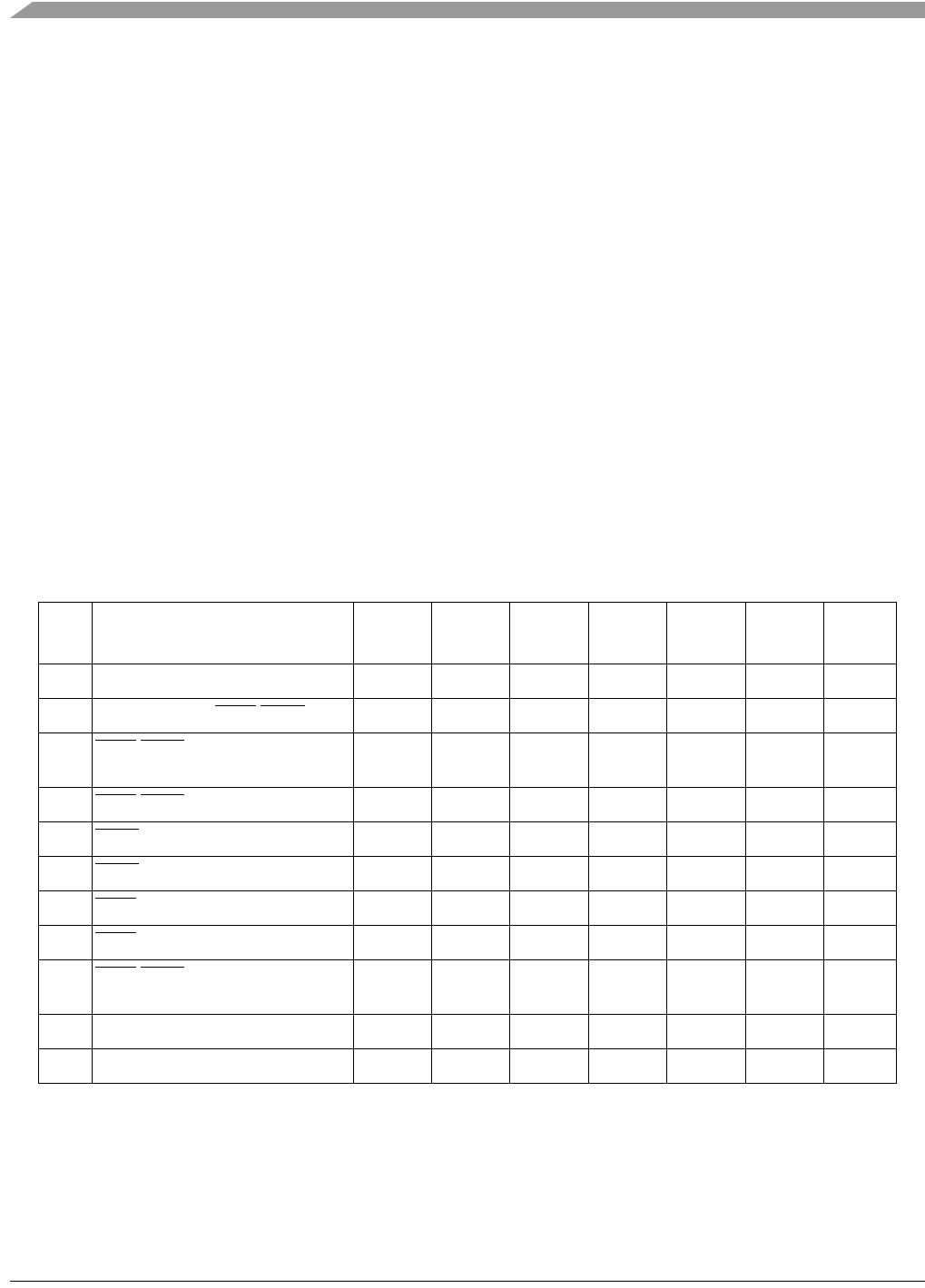
Table 27. PIO Mode Timing Specifications
Sym PIO Timing Parameter
Min/Max
(ns)
Mode 0
(ns)
Mode 1
(ns)
Mode 2
(ns)
Mode 3
(ns)
Mode 4
(ns)
SpecID
t
0
Cycle Time min 600 383 240 180 120 A8.1
t
1
Address valid to DIOR/DIOW setup min 70 50 30 30 25 A8.2
t
2
DIOR/DIOW pulse width 16-bit
8-bit
min
min
165
290
125
290
100
290
80
80
70
70
A8.3
t
2i
DIOR/DIOW recovery time min — — — 70 25 A8.4
t
3
DIOW data setup min 60 45 30 30 20 A8.5
t
4
DIOW data hold min 30 20 15 10 10 A8.6
t
5
DIOR data setup min 50 35 20 20 20 A8.7
t
6
DIOR data hold min55555A8.8
t
9
DIOR/DIOW to address
valid hold
min2015101010A8.9
t
A
IORDY setup max 35 35 35 35 35 A8.10
t
B
IORDY pulse width max 1250 1250 1250 1250 1250 A8.11


