MPC5200B Data Sheet, Rev. 1
Electrical and Thermal Characteristics
Freescale Semiconductor6
3 Electrical and Thermal Characteristics
3.1 DC Electrical Characteristics
3.1.1 Absolute Maximum Ratings
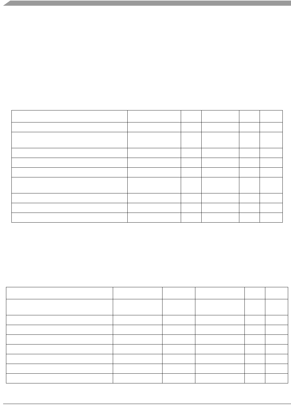
The tables in this section describe the MPC5200B DC Electrical characteristics. Table 1 gives the absolute
maximum ratings.
3.1.2 Recommended Operating Conditions
Table 2 gives the recommended operating conditions.
Table 1. Absolute Maximum Ratings
(1)
NOTES:
1
Absolute maximum ratings are stress ratings only, and functional operation at the maximums is not guaranteed.
Stresses beyond those listed may affect device reliability or cause permanent damage.
Characteristic Sym Min Max Unit SpecID
Supply voltage - e300 core and peripheral logic VDD_CORE –0.3 1.8 V D1.1
Supply voltage - I/O buffers VDD_IO,
VDD_MEM_IO
–0.3 3.6 V D1.2
Supply voltage - System APLL SYS_PLL_AVDD –0.3 2.1 V D1.3
Supply voltage - e300 APLL CORE_PLL_AVDD –0.3 2.1 V D1.4
Input voltage (VDD_IO) Vin –0.3 VDD_IO + 0.3 V D1.5
Input voltage (VDD_MEM_IO) Vin –0.3 VDD_MEM_IO
+ 0.3
V D1.6
Input voltage overshoot Vinos – 1.0 V D1.7
Input voltage undershoot Vinus – 1.0 V D1.8
Storage temperature range Tstg –55 150
o
C D1.9
Table 2. Recommended Operating Conditions
Characteristic Sym Min
(1)
Max
(1)
Unit SpecID
Supply voltage - e300 core and peripheral
logic
VDD_CORE 1.42 1.58 V D2.1
Supply voltage - standard I/O buffers VDD_IO 3.0 3.6 V D2.2
Supply voltage - memory I/O buffers (SDR) VDD_MEM_IO
SDR
3.0 3.6 V D2.3
Supply voltage - memory I/O buffers (DDR) VDD_MEM_IO
DDR
2.42 2.63 V D2.4
Supply voltage - System APLL SYS_PLL_AVDD 1.42 1.58 V D2.5
Supply voltage - e300 APLL CORE_PLL_AVDD 1.42 1.58 V D2.6
Input voltage - standard I/O buffers Vin 0 VDD_IO V D2.7
Input voltage - memory I/O buffers (SDR) Vin
SDR
0 VDD_MEM_IO
SDR
VD2.8


