Closed Dec 25th-26th
800-300-1968
We Stock Hard to Find Parts
My Account
|
My Orders
|
My Cart
Questions?
(800) 300-1968
Register
(current)
My Account
(current)
My Orders
(current)
My Cart
(current)
Categories
(current)
Manufacturers
Request a Quote
Sell Your Excess
Consignment
Quality Assurance
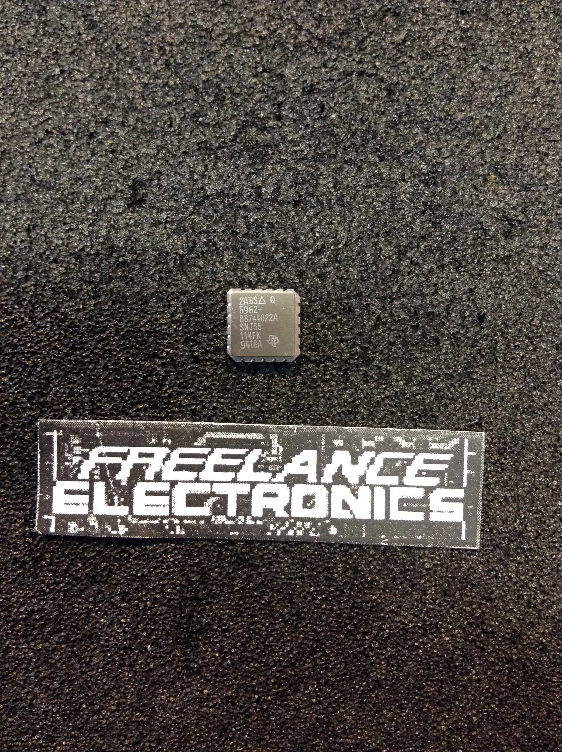
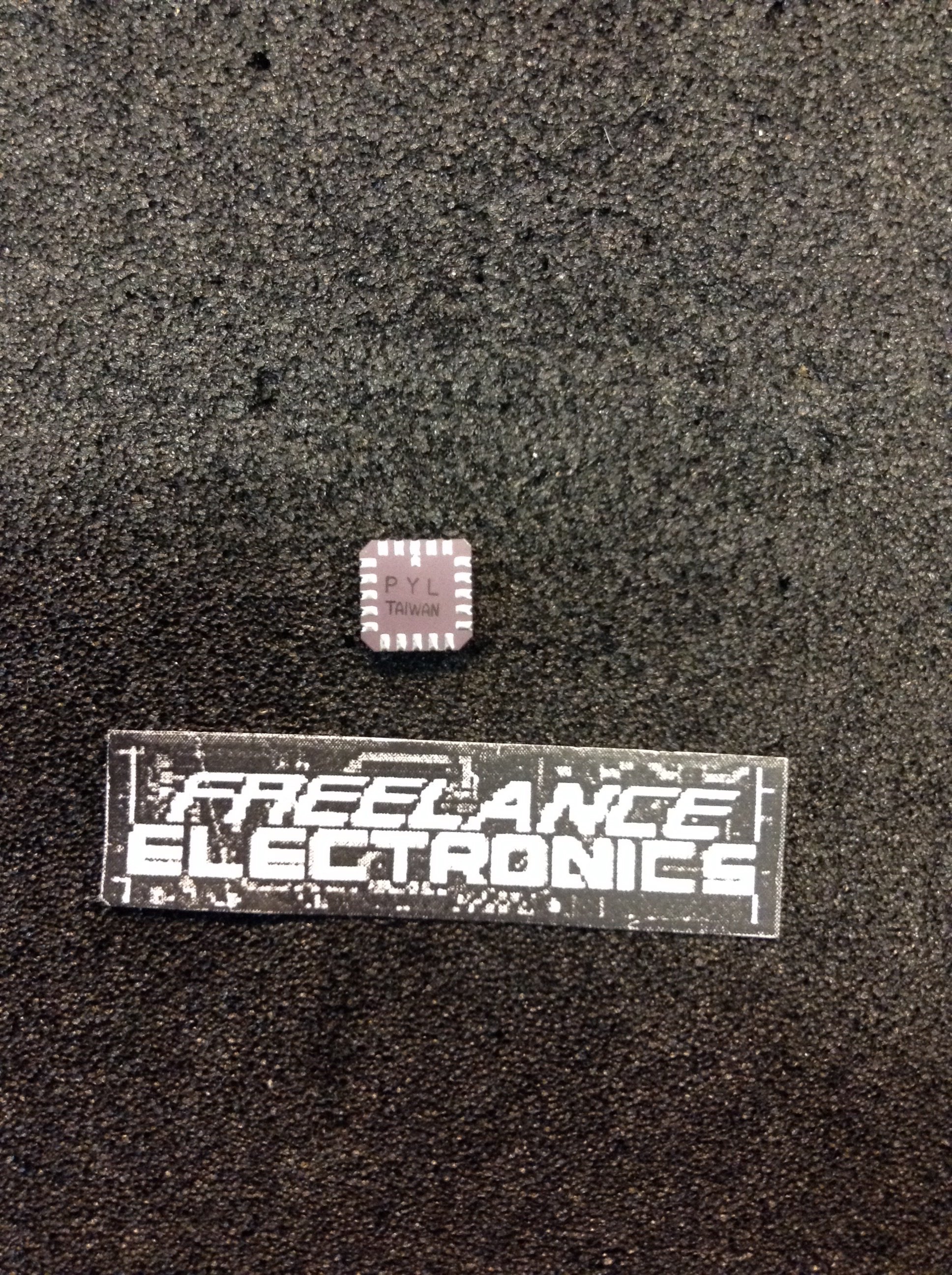
SNJ55114FK
Part #
SNJ55114FK
Description
Dual Transmitter 20-Pin CLLCCTube
Category
IC
Availability
In Stock
Qty
1
Qty
Price
1 +
$24.90162
Manufacturer
Available
Qty
Texas Instruments
Date Code: 9418
Freelance Stock:
1
Ships Immediately
Add to Cart
Related Items
Texas Instruments
IC
SNJ55107AFK
$51.96658
Texas Instruments
IC
SNJ55108AJ
$34.33012
Texas Instruments
IC
SNJ55109AJ
$16.07215
Texas Instruments
IC
SNJ55110AFK
$57.33213
Texas Instruments
IC
SNJ55110AJ
$16.67167
Texas Instruments
IC
SNJ55113J
$25.01293