SLLS266F − FEBRUARY 1997 − REVISED JULY 2004
FEATURES
D Design to Protect Submicron 3-V or 5-V
Circuits from Noise Transients
D Port ESD Protection Capability Exceeds:
− 15-kV Human Body Model
− 2-kV Machine Model
D Available in a WCSP Chip-Scale Package
D Stand-Off Voltage ...6.0 V Min
D Low Current Leakage ...1 µA Max at 6 V
D Low Capacitance ...35 pF Typ
DESCRIPTION
The SN65220 is a single transient voltage suppressor and
the SN65240 and SN75240 are dual transient voltage
suppressors designed to provide electrical noise transient
protection to Universal Serial Bus (USB) 1.1 ports. Note
that the input capacitance of the device makes it
unsuitable for high-speed USB 2.0 applications.
Any cabled I/O can be subjected to electrical noise
transients from various sources. These noise transients
can cause damage to the USB transceiver and/or the USB
ASIC if they are of sufficient magnitude and duration.
USB ports are typically implemented in 3-V or 5-V digital
CMOS with very limited ESD protection. The SN65220,
SN65240, and SN75240 can significantly increase the
port ESD protection level and reduce the risk of damage
to the circuits of the USB port.
The IEC1000-4-2 ESD performance of the SN65220,
SN65240, and SN75240 is measured at the system level.
Therefore, system design impacts the results of these
tests. A high compliance level may be attained with proper
board design and layout.
APPLICATIONS
D USB 1.1 Host, Hub, or Peripheral Ports
!" # $%&" !# '%()$!" *!"&+ *%$"#
$ " #'&$$!"# '& ",& "&# &-!# #"%&"# #"!*!* .!!"/+
*%$" '$&##0 *&# " &$&##!)/ $)%*& "&#"0 !)) '!!&"&#+
Please be aware that an important notice concerning availability, standard warranty, and use in critical applications of Texas Instruments
semiconductor products and disclaimers thereto appears at the end of this data sheet.
www.ti.com
Copyright 1997 − 2003, Texas Instruments Incorporated
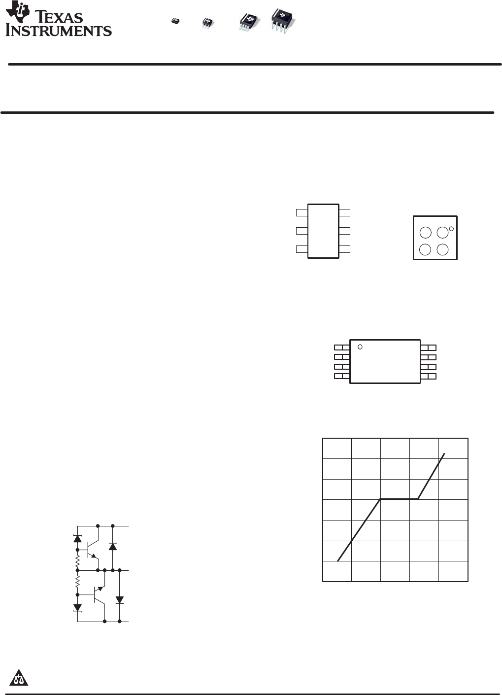
A1 A2
B2B1
A
GND
GND
B
SN65220YZB
(Size: 925 mm x 925 mm +6 mm)
(TOP VIEW)
3
2
4
6
(TOP VIEW)
†
1
NC
GND
NC
A
B
SN65220DBV
GND
5
NC − No internal connection
1
2
3
4
8
7
6
5
GND
C
GND
D
A
GND
B
GND
SN65240P, SN65240PW
SN75240P, SN75240PW
(TOP VIEW)
SADI
†
When read horizontally, Pin 1 is the bottom left pin.
NOTE A: Typical current versus voltage curve was derived
using the IEC 1.2/50-µs surge waveform.
CURRENT vs VOLTAGE
−2.5
−5
−7.5
−10
−5 0
0
2.5
5
5 10 15
Voltage − V
Current − A
−10
7.5
A or C
GND
B or D
(One Suppressor Shown)
NOTE
:
All GND terminals should be connected to ground.
EQUIVALENT SCHEMATIC DIAGRAM


