Closed Dec 25th-26th
800-300-1968
We Stock Hard to Find Parts
My Account
|
My Orders
|
My Cart
Questions?
(800) 300-1968
Register
(current)
My Account
(current)
My Orders
(current)
My Cart
(current)
Categories
(current)
Manufacturers
Request a Quote
Sell Your Excess
Consignment
Quality Assurance
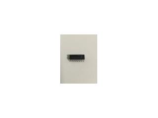
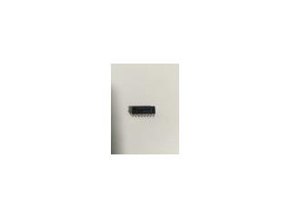
SN74LVCH322244AKR
Part #
SN74LVCH322244AKR
Description
IC BUFF/DVR TRI-ST 32BIT 96LFBGA
Category
IC
Availability
In Stock
Qty
37
Qty
Price
1 - 7
$5.17942
8 - 15
$4.11999
16 - 23
$3.88456
24 - 31
$3.60990
32 +
$3.21752
Manufacturer
Available
Qty
Texas Instruments
Freelance Stock:
20
Ships Immediately
Texas Instruments
Date Code: 0948
Freelance Stock:
17
Ships Immediately
Add to Cart
Related Items
Texas Instruments
IC
SN74L04J
$0.88396
Texas Instruments
IC
SN74L10N
$0.80361
Texas Instruments
IC
SN74L121N
$3.25729
Texas Instruments
IC
SN74L192N
$4.08183
Texas Instruments
IC
SN74L193N
$0.88396
Texas Instruments
IC
SN74L2279AN
$1.16683