5-557
FAST AND LS TTL DATA
QUAD 2-PORT REGISTER
The SN54/74LS398 and SN54/74LS399 are Quad 2-Port Registers. They
are the logical equivalent of a quad 2-input multiplexer followed by a quad 4-bit
edge-triggered register. A Common Select input selects between two 4-bit in-
put ports (data sources). The selected data is transferred to the output register
on the LOW-to-HIGH transition of the Clock input. The SN54/74LS398 fea-
tures both Q and Q
inputs, while the SN54/74LS399 has only Q outputs.
• Select From Two Data Sources
• Fully Positive Edge-Triggered Operation
• Both True and Complemented Outputs on SN54/74LS398
• Input Clamp Diodes Limit High-Speed Termination Effects
CONNECTION DIAGRAM DIP (TOP VIEW)
SN54/74LS398
SN54/74LS399
PIN NAMES LOADING (Note a)
HIGH
LOW
S Common Select Input 0.5 U.L. 0.25 U.L.
CP Clock (Active HIGH Going Edge) Input 0.5 U.L. 0.25 U.L.
I
0a
–I
0d
Data Inputs From Source 0 0.5 U.L. 0.25 U.L.
I
1a
–I
0d
Data Inputs From Source 1 0.5 U.L. 0.25 U.L.
Q
a
–Q
d
Register True Outputs (Note b) 10 U.L. 5 (2.5) U.L.
Q
a
–Q
d
Register Complementary Outputs
(Note b)
10 U.L. 5 (2.5) U.L.
NOTES:
a) 1 TTL Unit Load (U.L.) = 40 µA HIGH/1.6 mA LOW.
b) The Output LOW drive factor is 2.5 U.L. for Military (54) and 5 U.L. for Commercial
(74) Temperature Ranges.
SN54/74LS398
SN54/74LS399
QUAD 2-PORT REGISTER
LOW POWER SCHOTTKY
ORDERING INFORMATION
SN54LSXXXJ Ceramic
SN74LSXXXN Plastic
SN74LSXXXDW SOIC
SN74LSXXXD SOIC
J SUFFIX
CERAMIC
CASE 620-09
N SUFFIX
PLASTIC
CASE 648-08
16
1
16
1
16
1
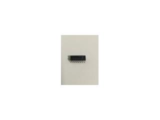
D SUFFIX
SOIC
CASE 751B-03
20
1
J SUFFIX
CERAMIC
CASE 732-03
20
1
N SUFFIX
PLASTIC
CASE 738-03
20
1
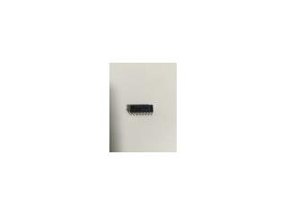
DW SUFFIX
SOIC
CASE 751D-03