5-473
FAST AND LS TTL DATA
QUAD 2-INPUT MULTIPLEXER
WITH STORAGE
The SN54/74LS298 is a Quad 2-Port Register. It is the logical equivalent of
a quad 2-input multiplexer followed by a quad 4-bit edge-triggered register. A
Common Select input selects between two 4-bit input ports (data sources.)
The selected data is transferred to the output register synchronous with the
HIGH to LOW transition of the Clock input.
The LS298 is fabricated with the Schottky barrier process for high speed
and is completely compatible with all Motorola TTL families.
• Select From Two Data Sources
• Fully Edge-Triggered Operation
• Typical Power Dissipation of 65 mW
• Input Clamp Diodes Limit High Speed Termination Effects
CONNECTION DIAGRAM DIP (TOP VIEW)
NOTE:
The Flatpak version
has the same pinouts
(Connection Diagram) as
the Dual In-Line Package.
PIN NAMES LOADING (Note a)
HIGH
LOW
S Common Select Input 0.5 U.L. 0.25 U.L.
CP Clock (Active LOW Going Edge) Input 0.5 U.L. 0.25 U.L.
I
0a
–I
0d
Data Inputs From Source 0 0.5 U.L. 0.25 U.L.
I
1a
–I
1d
Data Inputs From Source 1 0.5 U.L. 0.25 U.L.
Q
a
–Q
d
Register Outputs (Note b) 10 U.L. 5 (2.5) U.L.
NOTES:
a) 1 TTL Unit Load (U.L.) = 40 µA HIGH/1.6 mA LOW.
b) The Output LOW drive factor is 2.5 U.L. for Military (54) and 5 U.L. for Commercial
(74) Temperature Ranges.
SN54/74LS298
QUAD 2-INPUT MULTIPLEXER
WITH STORAGE
LOW POWER SCHOTTKY
ORDERING INFORMATION
SN54LSXXXJ Ceramic
SN74LSXXXN Plastic
SN74LSXXXD SOIC
J SUFFIX
CERAMIC
CASE 620-09
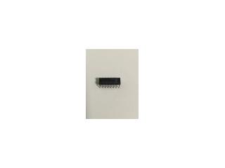
N SUFFIX
PLASTIC
CASE 648-08
16
1
16
1
16
1
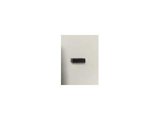
D SUFFIX
SOIC
CASE 751B-03
LOGIC SYMBOL