Closed Dec 25th-26th
800-300-1968
We Stock Hard to Find Parts
My Account
|
My Orders
|
My Cart
Questions?
(800) 300-1968
Register
(current)
My Account
(current)
My Orders
(current)
My Cart
(current)
Categories
(current)
Manufacturers
Request a Quote
Sell Your Excess
Consignment
Quality Assurance
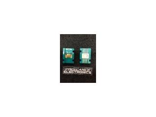
SN54LS75J
Part #
SN54LS75J
Description
Latch Transparent 4-CH D-Type16-Pin CDIP Tube
Category
IC
Availability
Out of Stock
Qty
0
Qty
Price
1 +
$10.09680
Related Items
Texas Instruments
IC
SN54L00R
$12.30486
Texas Instruments
IC
SN54L00T
$35.35877
Texas Instruments
IC
SN54L02J
$12.30486
Texas Instruments
IC
SN54L02T
$48.21648
Texas Instruments
IC
SN54L04FP
$12.30486
Texas Instruments
IC
SN54L04T
$9.32186