Closed Dec 25th-26th
800-300-1968
We Stock Hard to Find Parts
My Account
|
My Orders
|
My Cart
Questions?
(800) 300-1968
Register
(current)
My Account
(current)
My Orders
(current)
My Cart
(current)
Categories
(current)
Manufacturers
Request a Quote
Sell Your Excess
Consignment
Quality Assurance
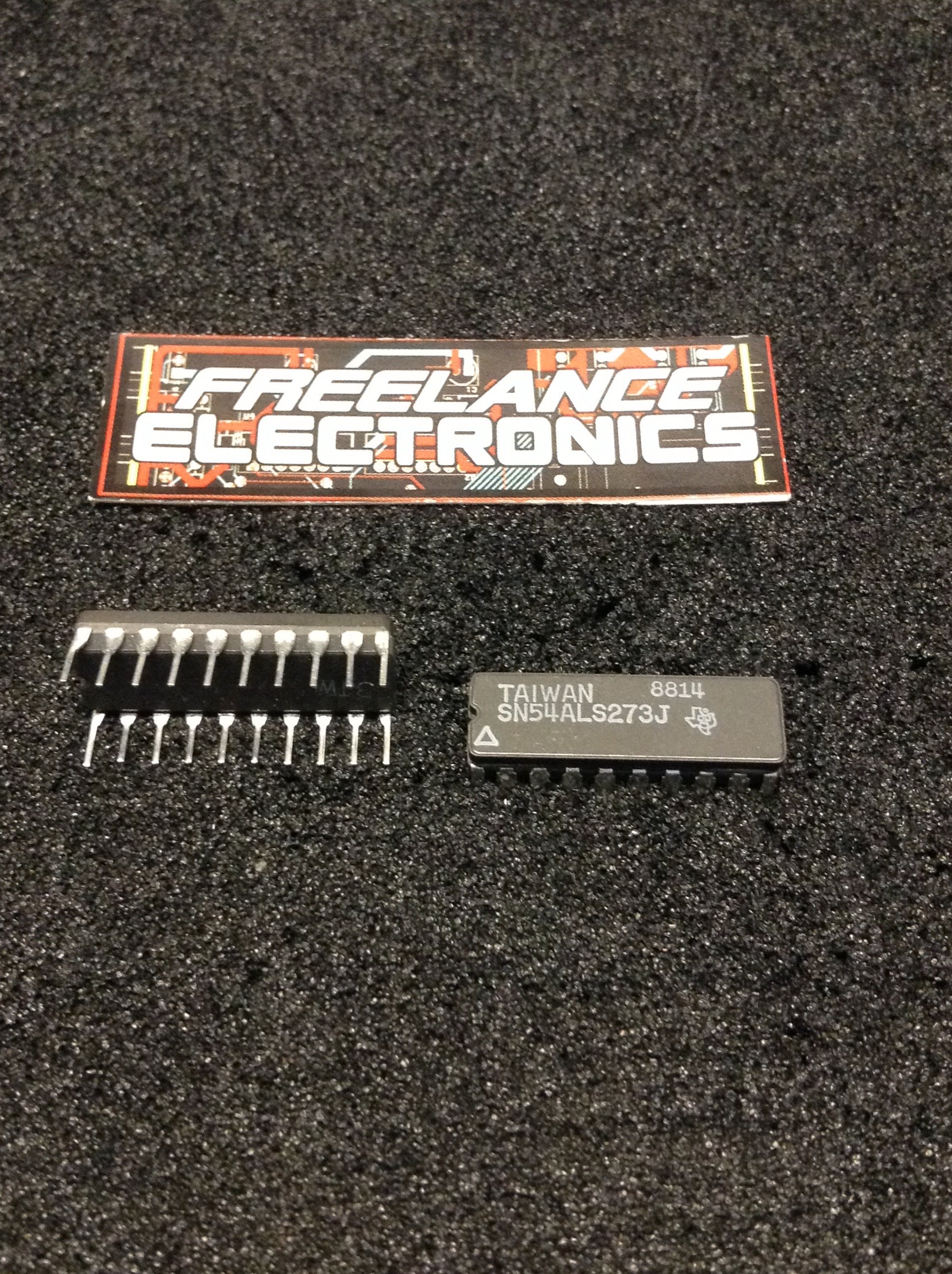
SN54ALS273J
Part #
SN54ALS273J
Description
OCTAL D-TYPE FLIP-FLOP, 20PIN CDIP
Category
IC
Availability
In Stock
Qty
23
Qty
Price
1 - 4
$13.04874
5 - 9
$10.37968
10 - 14
$9.78656
15 - 19
$9.09458
20 +
$8.10604
Manufacturer
Available
Qty
Texas Instruments
Date Code: 0618
Freelance Stock:
22
Ships Immediately
Texas Instruments
Date Code: 8814
Freelance Stock:
1
Ships Immediately
Add to Cart
Related Items
Texas Instruments
IC
SN54ABT3614HFP
$8.03608
Texas Instruments
IC
SN54ALS00AJ
$1.70462
Texas Instruments
IC
SN54ALS02J
$4.52030
Texas Instruments
IC
SN54ALS03BJ
$10.60763
Texas Instruments
IC
SN54ALS04AJ
$5.72813
Texas Instruments
IC
SN54ALS04BJ
$3.16815