Closed Dec 25th-26th
800-300-1968
We Stock Hard to Find Parts
My Account
|
My Orders
|
My Cart
Questions?
(800) 300-1968
Register
(current)
My Account
(current)
My Orders
(current)
My Cart
(current)
Categories
(current)
Manufacturers
Request a Quote
Sell Your Excess
Consignment
Quality Assurance
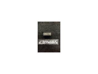
SN54221J
Part #
SN54221J
Description
DUAL MONOSTABLE MULTIVIBRATORS, 16PIN CDIP
Category
IC
Availability
In Stock
Qty
2
Qty
Price
1 +
$6.39332
Manufacturer
Available
Qty
Texas Instruments
Date Code: 8924
Freelance Stock:
2
Ships Immediately
Add to Cart
Related Items
Texas Instruments
IC
SN5420J
$12.68078
Texas Instruments
IC
SN5420W
$9.64330
Texas Instruments
IC
SN542759J
$16.97219
Texas Instruments
IC
SN54279W
$16.97219
Texas Instruments
IC
SN5428J
$18.20461
Motorola Corp
IC
SN542S00J
$16.97219