Freelance Electronics Components Distributor
Closed Dec 25th-26th
800-300-1968
We Stock Hard to Find Parts

SA5521N

Part # SA5521N
Description IC,LVDT CONDITIONER,BIPOLAR18Pin Plastic Dip
Category IC
Availability In Stock
Qty 305
Qty Price
1 - 3 $76.92905
4 - 8 $61.19356
9 - 17 $57.69678
18 - 37 $53.61721
38 + $47.78926
Manufacturer Available Qty
PHILLIPS COMPONENTS
Date Code: 0101
  • Shipping Freelance Stock: 2
    Ships Immediately
Philips Semiconductor
Date Code: 0101
  • Shipping Freelance Stock: 101
    Ships Immediately
Philips Semiconductor
Date Code: 0101
  • Shipping Freelance Stock: 47
    Ships Immediately
Philips Semiconductor
Date Code: 0101
  • Shipping Freelance Stock: 9
    Ships Immediately
Philips Semiconductor
Date Code: 0101
  • Shipping Freelance Stock: 28
    Ships Immediately
Philips Semiconductor
Date Code: 0101
  • Shipping Freelance Stock: 40
    Ships Immediately
Philips Semiconductor
Date Code: 0101
  • Shipping Freelance Stock: 73
    Ships Immediately
Philips Semiconductor
Date Code: 0101
  • Shipping Freelance Stock: 5
    Ships Immediately


Technical Document


DISCLAIMER: The information provided herein is solely for informational purposes. Customers must be aware of the suitability of this product for their application, and consider that variable factors such as Manufacturer, Product Category, Date Codes, Pictures and Descriptions may differ from available inventory.

Philips Semiconductors Linear Products Product specification
NE/SA/SE5521LVDT signal conditioner
901
August 31, 1994 853-0043 13721
DESCRIPTION
The NE/SA/SE5521 is a signal conditioning circuit for use with
Linear Variable Differential Transformers (LVDTs) and Rotary
Variable Differential Transformers (RVDTs). The chip includes a low
distortion, amplitude-stable sine wave oscillator with programmable
frequency to drive the primary of the LVDT/RVDT, a synchronous
demodulator to convert the LVDT/RVDT output amplitude and phase
to position information, and an output amplifier to provide
amplification and filtering of the demodulated signal.
FEATURES
Low distortion
Single supply 5V to 20V, or dual supply ±2.5V to ±10V
Oscillator frequency 1kHz to 20kHz
Capable of ratiometric operation
Low power consumption (182mV typ)
APPLICATIONS
LVDT signal conditioning
RVDT signal conditioning
LPDT signal conditioning
Bridge circuits
PIN CONFIGURATIONS
1
2
3
4
5
6
7
8
9
10
11
12
13
14
16
15
1
2
3
4
5
6
7
8
11
12
13
14
15
16
18
17
9
10
AMP OUT
+IN
–IN
LVDT IN
DEMOD OUT
SYNC
GND
N.C.
N.C.
V+
C
T
V
REF
FEEDBACK
OSC
OSC
V
REF/2
R
T
N.C.
AMP OUT
+IN
–IN
LVDT IN
DEMOD OUT
SYNC
GND
N.C.
V+
C
T
V
REF
FEEDBACK
OSC
OSC
V
REF/2
R
T
F, N Packages
TOP VIEW
D
1
Package
TOP VIEW
NOTE:
1. SOL — released in large SO package only.
ORDERING INFORMATION
DESCRIPTION TEMPERATURE RANGE ORDER CODE DWG #
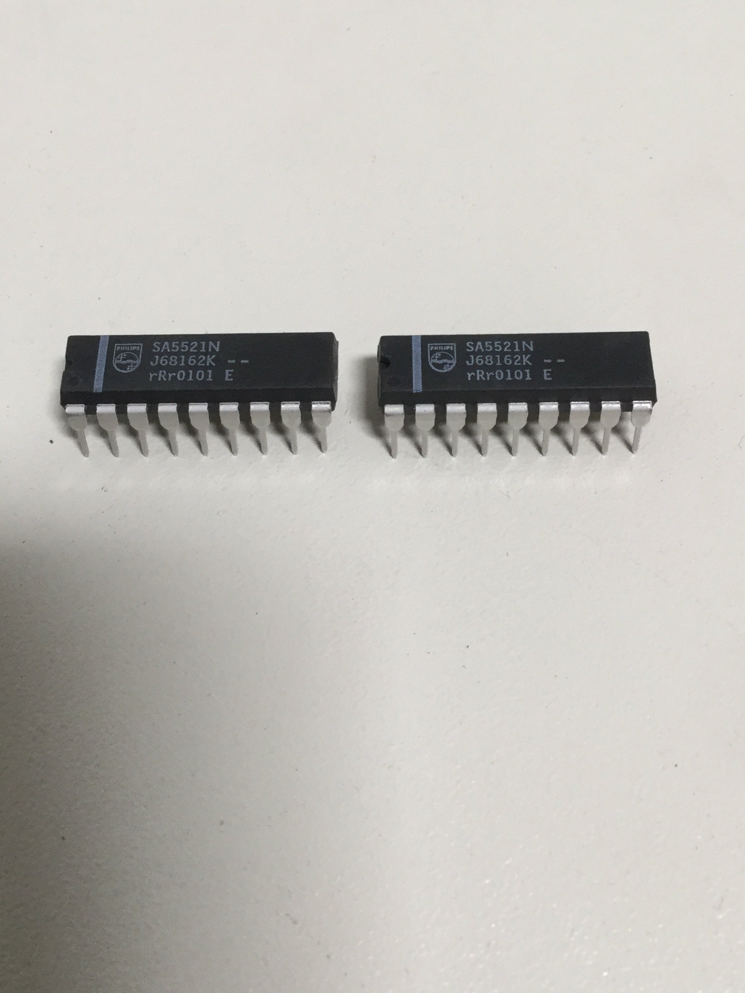
18-Pin Plastic Dual In-Line Package (DIP) 0 to +70°C NE5521N 0407A
16-Pin Small Outline Large (SOL) Package 0 to +70°C NE5521D 0171B
18-Pin Plastic Dual In-Line Package (DIP) –40 to +85°C SA5521N 0407A
18-Pin Ceramic Dual In-Line Package (CERDIP) –55 to +125°C SE5521F 0583A
16-Pin Ceramic Dual In-Line Package (CERDIP) –40 to +85°C SA5521D 0582B
ABSOLUTE MAXIMUM RATINGS
SYMBOL PARAMETER RATING UNIT
V
CC
Supply voltage +20 V
Split supply voltage ±10 V
T
A
Operating temperature range
NE5521
SA5521
SE5521
0 to 70
–40 to +85
–55 to +125
°C
°C
°C
T
STG
Storage temperature range –65 to +125 °C
P
D
Power dissipation
1
910 mW
NOTES:
1. For derating, see typical power dissipation versus load curves (Figure 1).
Philips Semiconductors Linear Products Product specification
NE/SA/SE5521LVDT signal conditioner
August 31, 1994
902
BLOCK DIAGRAM
NOTE:
Pin numbers are for F, N packages.
16
17
11
18
3
2
1
5
15
13
14
12
7
4
6
OSC
AUX AMP
DOMOD OUT
SINE
CONV
10k
10k
10k
10k
+
FEEDBACK
OSC
GND/V–
LVDT IN
SYNC
+
+
V
REF
V
REF
/2
OSC
C
T
R
T
V+
–IN
+IN
AMP
OUT
SYNCHRONOUS
DEMODULATOR
PIN DEFINITIONS FOR D, F AND N PACKAGES
PIN NO.
SYMBOL
DEFINITION
D F, N
SYMBOL
DEFINITION
1 1 Amp Out Auxiliary Amplifier Out.
2 2 +IN Auxiliary Amplifier non-inverting input.
3 3 –IN Auxiliary Amplifier inverting input.
4 4 LVDT IN Input to Synchronous Demodulator from the LVDT/RVDT secondary.
5 5 DEMOD OUT Pulsating DC output from the Synchronous Demodulator output. This voltage should be filtered before
use.
6 6 SYNC Synchronizing input for the Synchronizing Demodulator. This input should be connected to the OSC or
OSC
output. Sync is referenced to V
REF
/2.
7 7 GND Device return. Should be connected to system ground or to the negative supply.
8 8 NC No internal connection.
-- 9 NC No internal connection.
-- 10 NC No internal connection.
9 11 R
T
A temperature stable 18k resistor should be connected between this pin and Pin 7.
10 12 V
REF
/2 A high impedance source of one half the potential applied to V
REF
. The LVDT/RVDT secondary return
should be to this point. A bypass capacitor with low impedance at the oscillator frequency should also be
connected between this pin and ground.
11 13 OSC Oscillator sine wave output that is 180° out of phase with the OSC signal. The LVDT/RVDT primary is
usually connected between OSC and OSC
pins.
12 14 OSC Oscillator sine wave output. The LVDT/RVDT primaries are usually connected between OSC and OSC
pins.
13 15 FEEDBACK Usually connected to the OSC output for unity gain, a resistor between this pin and OSC, and one be-
tween this pin and ground can provide for a change in the oscillator output pin amplitudes.
14 16 V
REF
Reference voltage input for the oscillator and sine converter. This voltage MUST be stable and must not
exceed +V supply voltage.
15 17 C
T
Oscillator frequency-determining capacitor. The capacitor connected between this pin and ground should
be a temperature-stable type.
16 18 +V Positive supply connection.
Philips Semiconductors Linear Products Product specification
NE/SA/SE5521LVDT signal conditioner
August 31, 1994
903
DC ELECTRICAL CHARACTERISTICS
V+ = V
REF
= 10V, T
A
= 0 to 70°C for NE5521, T
A
= –55 to +125°C for SE5521, T
A
= –40 to 85°C for SA5521, Frequency = 1kHz, unless
otherwise noted.
SYMBOL
PARAMETER
TEST CONDITIONS
NE5521 SA/SE5521
UNIT
SYMBOL
PARAMETER
TEST CONDITIONS
Min Typ Max Min Typ Max
UNIT
V
CC
Supply current 12.9 20 12.9 18 mA
I
REF
Reference current 5.3 8 5.3 8 mA
V
REF
Reference voltage range 5 V+ 5 V+ V
P
D
Power dissipation 182 280 182 260 mW
Oscillator Section
Oscillator output R
L
= 10k
V
REF
8.8
V
REF
8.8
V
RMS
THD Sine wave distortion No load 1.5 1.5 %
Initial amplitude error T
A
= 25°C 0.4 ±3 0.4 ±3 %
Tempco of amplitude 0.005 0.01 0.005 0.01 %/°C
Init. accuracy of oscillator freq. T
A
= 25°C ±0.9 ±5 ±0.9 ±5 %
Temperature coeff. of frequency
1
0.05 0.05 %/°C
Voltage coeff. of frequency 2.5 3.3 %/V(V
REF
)
Min OSC (OSC) Load
2
300 170 300 170
Demodulator Section
r
Linearity error 5V
P-P
input ±0.05 ±0.1 ±0.05 ±0.1 %FS
Maximum demodulator input
V
REF
2
V
REF
2
V
P-P
V
OS
Demodulator offset voltage ±1.4 ±5 ±1.4 ±5 mV
TCV
OS
Demodulator offset voltage drift 5 25 5 25 µV/
5
C
I
BIAS
Demodulator input current –600 –234 –500 –234 nA
V
R/2
accuracy ±0.1 ±1 ±0.1 ±1 %
Auxiliary Output Amplifier
V
OS
Input offset voltage ±0.5 ±5 ±0.5 ±5 mV
I
BIAS
Input bias current –600 –210 –500 –210 nA
I
OS
Input offset current 10 50 10 50 nA
A
V
Gain 100 385 100 385 V/mV
SR Slew rate 1.3 1.3 V/µs
GBW Unity gain bandwidth product A
V
= 1 1.6 1.6 MHz
Output voltage swing R
L
= 10k 7 8.2 7 8.2 V
Output short circuit current to
ground or to V
CC
T
A
= 25°C 42 100 42 100 mA
NOTES:
1. This is temperature coefficient of frequency for the device only. It is assumed that C
T
and R
T
are fixed in value and C
T
leakage is fixed over
the operating temperature range.
2. Minimum load impedance for which distortion is guaranteed to be less than 5%.
12NEXT