Freelance Electronics Components Distributor
Closed Dec 25th-26th
800-300-1968
We Stock Hard to Find Parts

S29GL256N10TFI020

Part # S29GL256N10TFI020
Description NOR Flash Parallel 3.3V 256M-bit 32M x 8/16M x 16 100ns 56
Category IC
Availability In Stock
Qty 2
Qty Price
1 + $11.48011
Manufacturer Available Qty
Date Code: 0623
  • Shipping Freelance Stock: 2
    Ships Immediately


Technical Document


DISCLAIMER: The information provided herein is solely for informational purposes. Customers must be aware of the suitability of this product for their application, and consider that variable factors such as Manufacturer, Product Category, Date Codes, Pictures and Descriptions may differ from available inventory.

May 13, 2004 27631A4 S29GLxxxN MirrorBitTM Flash Family 97
Advance Information
AC Characteristics
OE#
CE#
Addresses
V
CC
WE#
Data
2AAh SA
t
AH
t
WP
t
WC
t
AS
t
WPH
555h for chip erase
10 for Chip Erase
30h
t
DS
t
VCS
t
CS
t
DH
55h
t
CH
In
Progress
Complete
t
WHWH2
VA
VA
Erase Command Sequence (last two cycles) Read Status Data
RY/BY#
t
RB
t
BUSY
Notes:
1. SA = sector address (for Sector Erase), VA = Valid Address for reading status data (see “Write Operation Status”.
2. These waveforms are for the word mode.
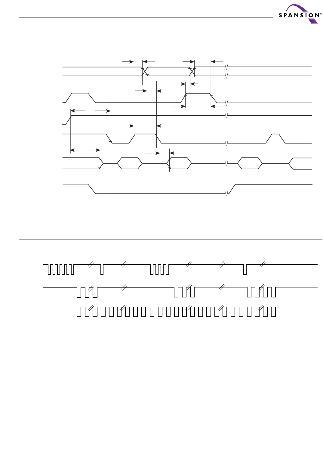
Figure 16. Chip/Sector Erase Operation Timings
98 S29GLxxxN MirrorBitTM Flash Family 27631A4 May 13, 2004
Advance Information
AC Characteristics
Figure 17. Data# Polling Timings
(During Embedded Algorithms)
WE#
CE#
OE#
High Z
t
OE
High Z
DQ7
DQ6–DQ0
RY/BY#
t
BUSY
Complement
Tr ue
Addresses
VA
t
OEH
t
CE
t
CH
t
OH
t
DF
VA VA
Status Data
Complement
Status Data
Tr ue
Valid Data
Valid Data
t
ACC
t
RC
Note:
1. VA = Valid address. Illustration shows first status cycle after command sequence, last status read cycle, and array data read
cycle.
2. t
OE
for data polling is 45 ns when V
IO
= 1.65 to 2.7 V and is 35 ns when V
IO
= 2.7 to 3.6 V
May 13, 2004 27631A4 S29GLxxxN MirrorBitTM Flash Family 99
Advance Information
AC Characteristics
OE#
CE#
WE#
Addresses
t
OEH
t
DH
t
AHT
t
ASO
t
OEPH
t
OE
Valid Data
(first read) (second read) (stops toggling)
t
CEPH
t
AHT
t
AS
DQ2 and DQ6 Valid Data
Valid
Status
Valid
Status
Valid
Status
RY/BY#
Note: VA = Valid address; not required for DQ6. Illustration shows first two status cycle after command
sequence, last status read cycle, and array data read cycle
Figure 18. Toggle Bit Timings (During Embedded Algorithms)
Note: DQ2 toggles only when read at an address within an erase-suspended sector. The system may use OE#
or CE# to toggle DQ2 and DQ6.
Figure 19. DQ2 vs. DQ6
Enter
Erase
Erase
Erase
Enter Erase
Suspend Program
Erase Suspend
Read
Erase Suspend
Read
Erase
WE#
DQ6
DQ2
Erase
Complete
Erase
Suspend
Suspend
Program
Resume
Embedded
Erasing
PREVIOUS262728293031323334353637NEXT