Closed Dec 25th-26th
800-300-1968
We Stock Hard to Find Parts
My Account
|
My Orders
|
My Cart
Questions?
(800) 300-1968
Register
(current)
My Account
(current)
My Orders
(current)
My Cart
(current)
Categories
(current)
Manufacturers
Request a Quote
Sell Your Excess
Consignment
Quality Assurance
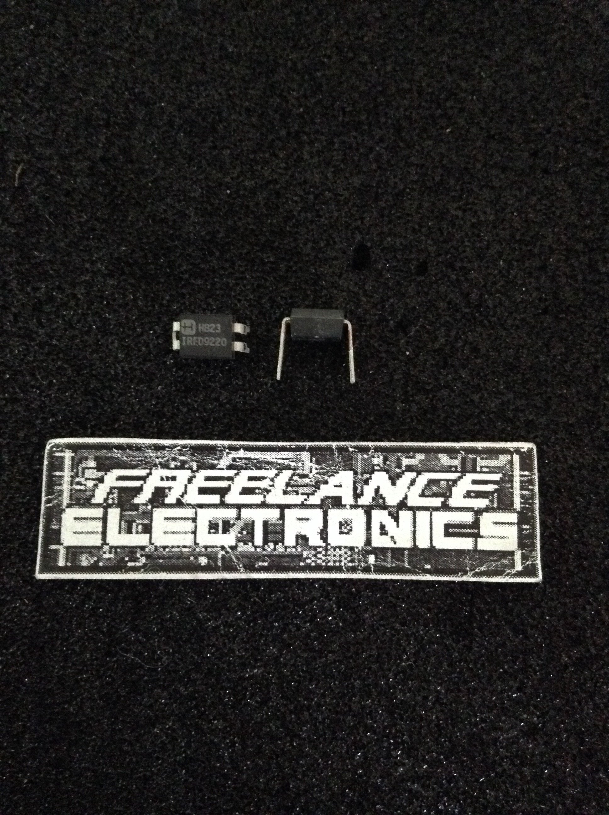
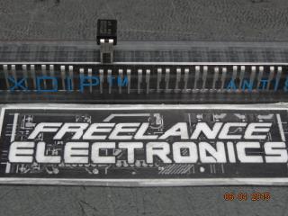
IRFD9220
Part #
IRFD9220
Description
MOSFET P-CH 200V 0.56A 4-DIP
Category
IC
Availability
In Stock
Qty
5
Qty
Price
1 +
$0.87668
Manufacturer
Available
Qty
Harris Corporation
Freelance Stock:
5
Ships Immediately
Add to Cart
Related Items
International Rectifier
TRANSISTOR
IRFD9020
$0.37963
International Rectifier
Microcircuit
IRFD9024
$1.80812
International Rectifier
IC
IRFD9110
$0.59231
Harris Corporation
TRANSISTOR
IRFD9113
$1.32327
Harris Corporation
RECTIFIER
IRFD9120
$0.20595
Harris Corporation
RECTIFIER
IRFD9123
$0.65749