Closed Dec 25th-26th
800-300-1968
We Stock Hard to Find Parts
My Account
|
My Orders
|
My Cart
Questions?
(800) 300-1968
Register
(current)
My Account
(current)
My Orders
(current)
My Cart
(current)
Categories
(current)
Manufacturers
Request a Quote
Sell Your Excess
Consignment
Quality Assurance
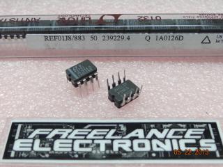
REF01HPZ
Part #
REF01HPZ
Description
IC PREC VOLT REFERENCE 10V 8-DIP
Category
IC
Availability
Out of Stock
Qty
0
Qty
Price
1 +
$2.64391
Related Items
PMI
IC
REF01CP
$1.15208
Analog Devices
IC
REF01CS
$2.19867
PMI
IC
REF01EZ
$10.04289
Analog Devices
IC
REF01HP
$2.04555
Linear Technology
IC
REF01J8/883
$25.65116
Linear Technology
IC
REF01J8/883C