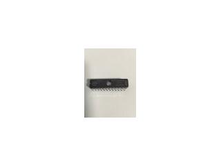
Freelance Electronics Components Distributor
Closed Dec 25th-26th
800-300-1968
We Stock Hard to Find Parts

PLDC20G10-30LMB

Part # PLDC20G10-30LMB
Description SPLD PLDC20G10 Family 400 Gates 10 Macro Cells 31.25MHz 5V
Category IC
Availability In Stock
Qty 8
Qty Price
1 - 1 $81.73837
2 - 3 $65.01916
4 - 5 $61.30378
6 - 6 $56.96917
7 + $50.77687
Manufacturer Available Qty
CYPRESS SEMICONDUCTOR
Date Code: 8652
  • Shipping Freelance Stock: 8
    Ships Immediately


Technical Document


DISCLAIMER: The information provided herein is solely for informational purposes. Customers must be aware of the suitability of this product for their application, and consider that variable factors such as Manufacturer, Product Category, Date Codes, Pictures and Descriptions may differ from available inventory.

USE ULTRA37000™ FOR
ALL NEW DESIGNS
CMOS Generic 24-Pin Reprogrammable
Logic Device
PLDC20G10B
PLDC20G10
Cypress Semiconductor Corporation 3901 North First Street San Jose, CA 95134 408-943-2600
Document #: 38-03010 Rev. *A Revised April 20, 2004
Features
Fast
Commercial: t
PD
= 15 ns, t
CO
= 10 ns, t
S
= 12 ns
Military: t
PD
= 20 ns, t
CO
= 15 ns, t
S
= 15 ns
•Low power
—I
CC
max.: 70 mA, commercial
—I
CC
max.: 100 mA, military
Commercial and military temperature range
User-programmable output cells
Selectable for registered or combinatorial operation
Output polarity control
Output enable source selectable from pin 13 or
product term
Generic architecture to replace standard logic
functions including: 20L10, 20L8, 20R8, 20R6, 20R4,
12L10, 14L8, 16L6, 18L4, 20L2, and 20V8
Eight product terms and one OE product term per output
CMOS EPROM technology for reprogrammability
Highly reliable
Uses proven EPROM technology
Fully AC and DC tested
Security feature prevents logic pattern duplication
±10% power supply voltage and higher noise
immunity
Functional Description
Cypress PLD devices are high-speed electrically program-
mable logic devices. These devices utilize the sum-of-products
(AND-OR) structure providing users the ability to program
custom logic functions for unique requirements.
In an unprogrammed state the AND gates are connected via
EPROM cells to both the true and complement of every input.
By selectively programming the EPROM cells, AND gates may
be connected to either the true or complement or disconnected
from both true and complement inputs.
Note:
1. The CG7C323 is the PLDC20G10 packaged in the JEDEC-compatible 28-pin PLCC pinout. Pin function and pin order is identical for both PLCC pinouts. The
difference is in the location of the “no connect” or NC pins.
Logic Block Diagram
PinConfigurations
8
987654321
10
15
16
17
18 19 20 21 22 23 24
PROGRAMMABLE
ANDARRAY
IIIIIIIICP/I
OUTPUT
CELL
8
OUTPUT
CELL
8
OUTPUT
CELL
OE
OE
OE
8
OE
OUTPUT
CELL
8
OE
OUTPUT
CELL
8
OE
OUTPUT
CELL
8
OE
OUTPUT
CELL
8
OE
OUTPUT
CELL
V
CC
11
12
13 14
I
V
SS
I/OE
8
OUTPUT
CELL
8
OUTPUT
CELL
I
I/O
9
I/O
8
I/O
7
I/O
6
I/O
5
I/O
4
I/O
3
I/O
2
I/O
1
I/O
0
5
6
7
8
9
10
11
4 3 2 282726
12131415161718
25
24
23
22
21
20
19
I
I
I
I
I
NC
25
24
23
22
21
20
19
5
6
7
8
9
10
11
121314 1516 1718
432 282726
I
I
I
I
I
I
NC
9
I
I
V
I/O
I/O
8
I/O
I/O
V
I
I
SS
I
I
CP/I
V
I/O
I/O
0
1
0
1
CC
CC
9
8
I/O
I/O
V
I
I
SS
1
1
CP/I
NC
I
I/O
2
I/O
3
I/O
4
I/O
5
I/O
6
I/O
7
NC
I/OE
NC
PLDC20G10
PLDC20G10B
25
24
23
22
21
20
19
5
6
7
8
9
10
11
121314 1516 1718
4 3 2 2827 26
NC
I
I
I
I
NC
I
I
CP/I
V
I/O
I/O
0
1
CC
9
8
I/O
I/O
I
I
1
V
SS
I
NC
I
I/OE
I/O
2
I/O
3
I/O
4
I/O
5
I/O
6
I/O
7
NC
JEDEC PLCC
Top View
STD PLCC
Top View
LCC
Top View
I/O
2
I/O
3
I/O
4
I/O
5
I/O
6
I/O
7
NC
NC
I/OE
PLDC20G10
PLDC20G10B
CG7C323–A
CG7C323B–A
NC
[1]
USE ULTRA37000™ FOR
ALL NEW DESIGNS
PLDC20G10B
PLDC20G10
Document #: 38-03010 Rev. *A Page 2 of 14
Functional Description
Cypress PLDC20G10 uses an advanced 0.8-micron CMOS
technology and a proven EPROM cell as the programmable
element. This technology and the inherent advantage of being
able to program and erase each cell enhances the reliability
and testability of the circuit. This reduces the burden on the
customer to test and to handle rejects.
A preload function allows the registered outputs to be preset
to any pattern during testing. Preload is important for testing
the functionality of the Cypress PLD device.
20G10 Functional Description
The PLDC20G10 is a generic 24-pin device that can be
programmed to logic functions that include but are not limited
to: 20L10, 20L8, 20R8, 20R6, 20R4, 12L10, 14L8, 16L6, 18L4,
20L2, and 20V8. Thus, the PLDC20G10 provides significant
design, inventory and programming flexibility over dedicated
24-pin devices. It is executed in a 24-pin 300-mil molded DIP
and a 300-mil windowed cerDIP. It provides up to 22 inputs and
10 outputs. When the windowed cerDIP is exposed to UV light,
the 20G10 is erased and then can be reprogrammed.
The programmable output cell provides the capability of
defining the architecture of each output individually. Each of
the 10 output cells may be configured with registered or combi-
natorial outputs, active HIGH or active LOW outputs, and
product term or Pin 13 generated output enables. Three archi-
tecture bits determine the configurations as shown in the
Configuration Table and in Figures 1 through 8. A total of eight
different configurations are possible, with the two most
common shown in Figure 3 and Figure 5. The default or unpro-
grammed state is registered/active/LOW/Pin 11 OE. The
entire programmable output cell is shown in the next section.
The architecture bit ‘C1’ controls the registered/combinatorial
option. In either combinatorial or registered configuration, the
output can serve as an I/O pin, or if the output is disabled, as
an input only. Any unused inputs should be tied to ground. In
either registered or combinatorial configuration, the output of
the register is fed back to the array. This allows the creation of
control-state machines by providing the next state. The
register is clocked by the signal from Pin 1. The register is
initialized on power up to Q
output LOW and Q output HIGH.
In both the combinatorial and registered configurations, the
source of the output enable signal can be individually chosen
with architecture bit ‘C2’. The OE signal may be generated
within the array, or from the external OE
(Pin 13). The Pin 13
allows direct control of the outputs, hence having faster
enable/disable times.
Each output cell can be configured for output polarity. The
output can be either active HIGH or active LOW. This option is
controlled by architecture bit ‘C0’.
Along with this increase in functional density, the Cypress
PLDC20G10 provides lower-power operation through the use
of CMOS technology and increased testability with a register
preload feature.
Selection Guide
I
CC
(mA) t
PD
(ns) t
S
(ns) t
CO
(ns)
Generic
Part Number Com/Ind Mil Com/Ind Mil Com/Ind Mil Com/Ind Mil
20G10B–15 70 15 12 10
20G10B–20 70 100 20 20 12 15 12 15
20G10B–25 100 25 18 15
20G10–25 55 25 15 15
20G10–30 80 30 20 20
20G10–35 55 35 30 25
20G10–40 80 40 35 25
USE ULTRA37000™ FOR
ALL NEW DESIGNS
PLDC20G10B
PLDC20G10
Document #: 38-03010 Rev. *A Page 3 of 14
Programmable Output Cell
Configuration Table
Figure C
2
C
1
C
0
Configuration
1 0 0 0 Product Term OE/Registered/Active LOW
2 0 0 1 Product Term OE/Registered/Active HIGH
5 0 1 0 Product Term OE/Combinatorial/Active LOW
6 0 1 1 Product Term OE/Combinatorial/Active HIGH
3 1 0 0 Pin 13 OE/Registered/Active LOW
4 1 0 1 Pin 13 OE/Registered/Active HIGH
7 1 1 0 Pin 13 OE/Combinatorial/Active LOW
8 1 1 1 Pin 13 OE/Combinatorial/Active HIGH
OUTPUT
SELECT
MUX
C
1
C
0
Q
QD
CP
INPUT/
FEED–
BACK
MUX
C
3
C
1
01
00
11
10
0
1
C
0
C
2
OUTPUT
ENABLE
MUX
C
2
PIN 13
OE PRODUCT
TERM
Registered Output Configurations
Figure 1. Product Term OE/Active LOW Figure 2. Product Term OE/Active HIGH
Figure 3. Pin 13 OE/Active LOW Figure 4. Pin 13 OE/Active HIGH
Q
QD
CP
C
2
=0
C
1
=0
C
0
=0
Q
QD
CP
C
2
=0
C
1
=0
C
0
=1
Q
QD
CP
C
2
=1
C
1
=0
C
0
= 0
Q
QD
CP
C
2
=1
C
1
=0
C
0
=1
12345NEXT