Freelance Electronics Components Distributor
Closed Dec 25th-26th
800-300-1968
We Stock Hard to Find Parts

PCI1510GGU

Part # PCI1510GGU
Description PCI TO PC CARD CONTROLLER - Trays
Category IC
Availability Out of Stock
Qty 0
Qty Price
1 + $3.74600


Technical Document


DISCLAIMER: The information provided herein is solely for informational purposes. Customers must be aware of the suitability of this product for their application, and consider that variable factors such as Manufacturer, Product Category, Date Codes, Pictures and Descriptions may differ from available inventory.

5−19
5.21 ExCA I/O Windows 0 and 1 Offset-Address Low-Byte Registers
These registers contain the low byte of the 16-bit I/O window offset address for I/O windows 0 and 1. The 8 bits of
these registers correspond to the lower 8 bits of the offset address, and bit 0 is always 0b.
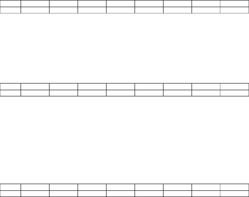
Bit 7 6 5 4 3 2 1 0
Default 0 0 0 0 0 0 0 0
Register: ExCA I/O window 0 offset-address low-byte
Offset: CardBus socket address + 836h; ExCA offset 36h
Register: ExCA I/O window 1 offset-address low-byte
Offset: CardBus socket address + 838h; ExCA offset 38h
Type: Read-only, Read/Write
Default: 00h
5.22 ExCA I/O Windows 0 and 1 Offset-Address High-Byte Registers
These registers contain the high byte of the 16-bit I/O window offset address for I/O windows 0 and 1. The 8 bits of
these registers correspond to the upper 8 bits of the offset address.
Bit 7 6 5 4 3 2 1 0
Default 0 0 0 0 0 0 0 0
Register: ExCA I/O window 0 offset-address high-byte
Offset: CardBus socket address + 837h; ExCA offset 37h
Register: ExCA I/O window 1 offset-address high-byte
Offset: CardBus socket address + 839h; ExCA offset 39h
Type: Read/Write
Default: 00h
5.23 ExCA Memory Windows 0−4 Page Registers
The upper 8 bits of a 4-byte PCI memory address are compared to the contents of this register when decoding
addresses for 16-bit memory windows. Each window has its own page register, all of which default to 00h. By
programming this register to a nonzero value, host software can locate 16-bit memory windows in any 1 of 256
16-Mbyte regions in the 4-Gbyte PCI address space. These registers are only accessible when the ExCA registers
are memory-mapped; that is, these registers cannot be accessed using the index/data I/O scheme.
Bit 7 6 5 4 3 2 1 0
Default 0 0 0 0 0 0 0 0
Register: ExCA memory windows 0−4 page
Offset: CardBus socket address + 840h, 841h, 842h, 843h, 844h
Type: Read/Write
Default: 00h
5−20
6−1
6 CardBus Socket Registers
The PC Card Standard requires a CardBus socket controller to provide five 32-bit registers that report and control
socket-specific functions. The PCI1510 controller provides the CardBus socket/ExCA base-address register (PCI
offset 10h, see Section 4.12) to locate these CardBus socket registers in PCI memory address space. Table 6−1 gives
the location of the socket registers in relation to the CardBus socket/ExCA base address.
The controller implements an additional register at offset 20h that provides power management control for the socket.
CardBus Socket/ExCA Base Address
16-Bit Legacy-Mode Base Address
10h
44h
PCI1510 Configuration Registers
CardBus
Socket
Registers
Host
Memory Space
00h
ExCA
Registers
20h
800h
844h
OffsetOffset
Figure 6−1. Accessing CardBus Socket Registers Through PCI Memory
Table 6−1. CardBus Socket Registers
REGISTER NAME OFFSET
Socket event 00h
Socket mask 04h
Socket present-state 08h
Socket force event 0Ch
Socket control 10h
Reserved 14h−1Ch
Socket power-management 20h
A bit description table, typically included when a register contains bits of more than one type or purpose, indicates
bit field names, which appear in the signal column; a detailed field description, which appears in the function column;
and field access tags, which appear in the type column of the bit description table. Table 4−2 describes the field
access tags.
PREVIOUS3031323334353637383940414243NEXT