4−29
4.48 Serial-Bus Control and Status Register
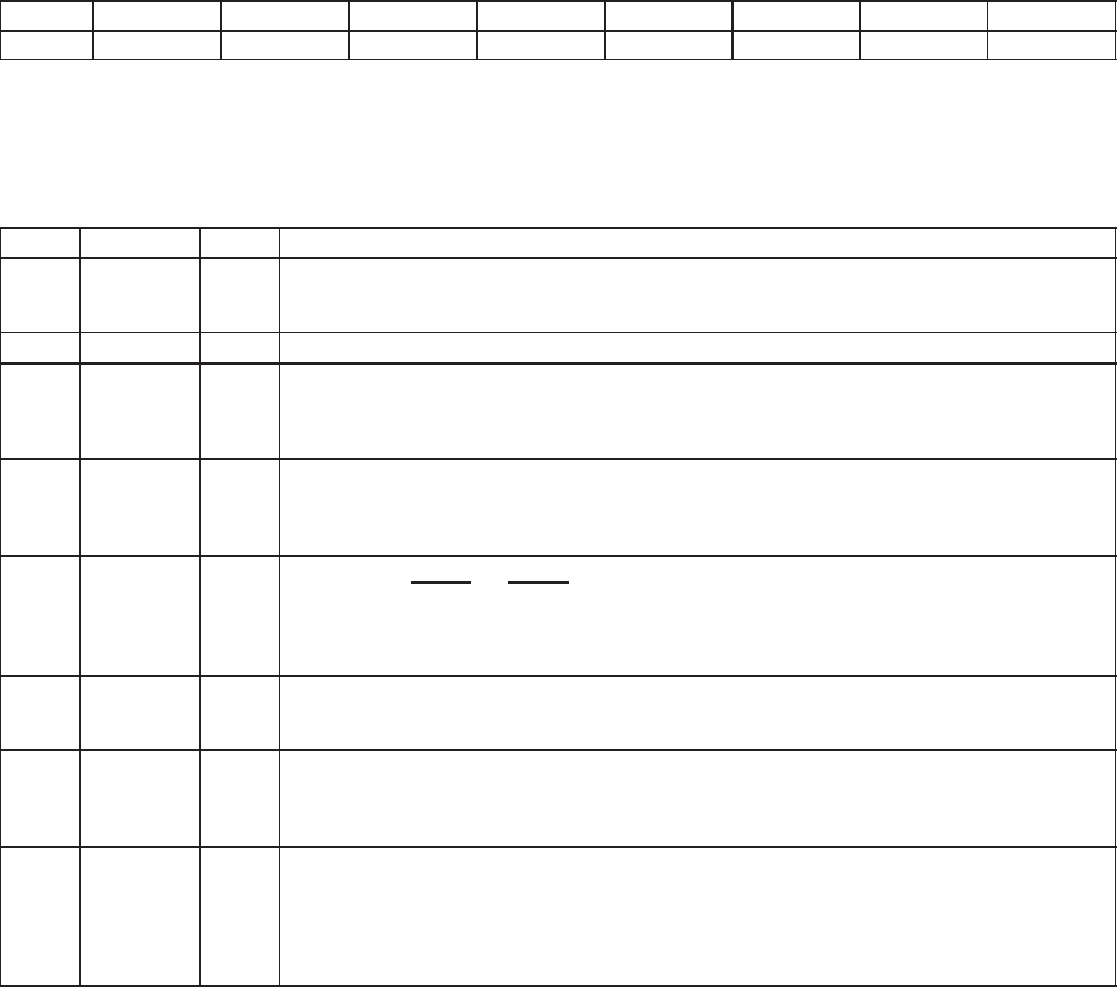
The serial-bus control and status register communicates serial-bus status information and selects the quick
command protocol. Bit 5 (REQBUSY) in this register must be polled during serial-bus byte reads to indicate when
data is valid in the serial-bus data register. See Table 4−23 for a complete description of the register contents.
Bit 7 6 5 4 3 2 1 0
Default 0 0 0 0 0 0 0 0
Register: Serial-bus control and status
Offset: B3h (function 0)
Type: Read-only, Read/Write, Read/Clear
Default: 00h
Table 4−23. Serial-Bus Control and Status Register Description
BIT SIGNAL TYPE FUNCTION
7 PROT_SEL RW
Protocol select. When bit 7 is set, the send-byte protocol is used on write requests and the receive-byte
protocol is used on read commands. The word-address byte in the serial-bus index register (PCI offset B1h,
see Section 4.46) is not output by the controller when bit 7 is set.
6 RSVD R Reserved. Bit 6 returns 0b when read.
5 REQBUSY R
Requested serial-bus access busy. Bit 5 indicates that a requested serial-bus access (byte read or write)
is in progress. A request is made, and bit 5 is set, by writing to the serial-bus slave address register (PCI
offset B2h, see Section 4.47). Bit 5 must be polled on reads from the serial interface. After the byte read
access has been requested, the read data is valid in the serial-bus data register.
4 ROMBUSY R
Serial EEPROM busy status. Bit 4 indicates the status of the serial EEPROM circuitry. Bit 4 is set during
the loading of the subsystem ID and other default values from the serial-bus EEPROM.
0 = Serial EEPROM circuitry is not busy
1 = Serial EEPROM circuitry is busy
3 SBDETECT RC
Serial-bus detect. When bit 3 is set, it indicates that the serial-bus interface is detected through pullup
resistors on the VCCD0
and VCCD1 terminals after reset. If bit 3 is reset, then the MFUNC4 and MFUNC1
terminals can be used for alternate functions such as general-purpose inputs and outputs.
0 = Serial-bus interface not detected
1 = Serial-bus interface detected
2 SBTEST RW
Serial-bus test. When bit 2 is set, the serial-bus clock frequency is increased for test purposes.
0 = Serial-bus clock at normal operating frequency, 100 kHz (default)
1 = Serial-bus clock frequency increased for test purposes
1 REQ_ERR RC
Requested serial-bus access error. Bit 1 indicates when a data error occurs on the serial interface during
a requested cycle, and can be set due to a missing acknowledge. Bit 1 is cleared by a writeback of 1b.
0 = No error detected during user-requested byte read or write cycle
1 = Data error detected during user-requested byte read or write cycle
0 ROM_ERR RC
EEPROM data-error status. Bit 0 indicates when a data error occurs on the serial interface during the
auto-load from the serial-bus EEPROM, and can be set due to a missing acknowledge. Bit 0 is also set on
invalid EEPROM data formats. See Section 3.6.1, Serial Bus Interface Implementation, for details on
EEPROM data format. Bit 0 is cleared by a writeback of 1b.
0 = No error detected during auto-load from serial-bus EEPROM
1 = Data error detected during auto-load from serial-bus EEPROM

