Freelance Electronics Components Distributor
Closed Dec 25th-26th
800-300-1968
We Stock Hard to Find Parts

PCI1510GGU

Part # PCI1510GGU
Description PCI TO PC CARD CONTROLLER - Trays
Category IC
Availability Out of Stock
Qty 0
Qty Price
1 + $3.74600


Technical Document


DISCLAIMER: The information provided herein is solely for informational purposes. Customers must be aware of the suitability of this product for their application, and consider that variable factors such as Manufacturer, Product Category, Date Codes, Pictures and Descriptions may differ from available inventory.

4−19
4.33 Device Control Register
The device control register is provided for PCI1130 compatibility. See Table 4−11 for a complete description of the
register contents.
Bit 7 6 5 4 3 2 1 0
Default 0 1 1 0 0 1 1 0
Register: Device control
Offset: 92h
Type: Read-only, Read/Write
Default: 66h
Table 4−11. Device Control Register Description
BIT SIGNAL TYPE FUNCTION
7 SKTPWR_LOCK RW
Socket power lock bit. When this bit is set to 1b, software cannot power down the PC Card socket while
in D3. This may be necessary to support wake on LAN or RING if the operating system is programmed
to power down a socket when the CardBus controller is placed in the D3 state.
6 3VCAPABLE RW
3-V socket capable force
0 = Not 3-V capable
1 = 3-V capable (default)
5 IO16V2 RW Diagnostic bit. This bit defaults to 1b.
4 RSVD R Reserved. Bit 4 returns 0b when read.
3 TEST RW TI test. Only a 0b should be written to bit 3.
2−1 INTMODE RW
Interrupt signaling mode. Bits 2 and 1 select the interrupt signaling mode. The interrupt signaling
mode bits are encoded:
00 = Parallel PCI interrupts only
01 = Parallel IRQ and parallel PCI interrupts
10 = IRQ serialized interrupts and parallel PCI interrupt
11 = IRQ and PCI serialized interrupts (default)
0 RSVD RW Reserved. Bit 0 is reserved for test purposes. Only 0b should be written to this bit.
4−20
4.34 Diagnostic Register
The diagnostic register is provided for internal TI test purposes. It is a read/write register, but only 00h should be
written to it. See Table 4−12 for a complete description of the register contents.
Bit 7 6 5 4 3 2 1 0
Default 0 1 1 0 0 0 0 0
Register: Diagnostic
Offset: 93h
Type: Read/Write
Default: 60h
Table 4−12. Diagnostic Register Description
BIT SIGNAL TYPE FUNCTION
7 TRUE_VAL RW
This bit defaults to 0b. This bit is encoded as:
0 = Reads true values in PCI vendor ID and PCI device ID registers (default)
1 = Reads all 1s in reads from the PCI vendor ID and PCI device ID registers
6 RSVD R Reserved. Bit 6 returns 1b when read.
5 CSC RW
CSC interrupt routing control
0 = CSC interrupts routed to PCI if ExCA 803 bit 4 = 1b
1 = CSC interrupts routed to PCI if ExCA 805 bits 7−4 = 0000b (default)
In this case, the setting of ExCA 803 bit 4 is a don’t care.
4 DIAG4 RW Diagnostic RETRY_DIS. Delayed transaction disable.
3 DIAG3 RW Diagnostic RETRY_EXT. Extends the latency from 16 to 64.
2 DIAG2 RW Diagnostic DISCARD_TIM_SEL_CB. Set = 2
10
, reset = 2
15
.
1 DIAG1 RW Diagnostic DISCARD_TIM_SEL_PCI. Set = 2
10
, reset = 2
15
.
0 STDZVEN RW
Standardized zoomed video register model enable.
0 = Enable the standardized zoomed video register model (default)
1 = Disable the standardized zoomed video register model
4.35 Capability ID Register
The capability ID register identifies the linked list item as the register for PCI power management. The register returns
01h when read, which is the unique ID assigned by the PCI SIG for the PCI location of the capabilities pointer and
the value.
Bit 7 6 5 4 3 2 1 0
Default 0 0 0 0 0 0 0 1
Register: Capability ID
Offset: A0h
Type: Read-only
Default: 01h
4.36 Next-Item Pointer Register
The next-item pointer register indicates the next item in the linked list of the PCI power-management capabilities.
Because the controller function includes only one capabilities item, this register returns 00h when read.
Bit 7 6 5 4 3 2 1 0
Default 0 0 0 0 0 0 0 0
Register: Next-item pointer
Offset: A1h
Type: Read-only
Default: 00h
4−21
4.37 Power-Management Capabilities Register
This register contains information on the capabilities of the PC Card function related to power management. The
CardBus bridge supports the D0, D1, D2, and D3 power states. See Table 4−13 for a complete description of the
register contents.
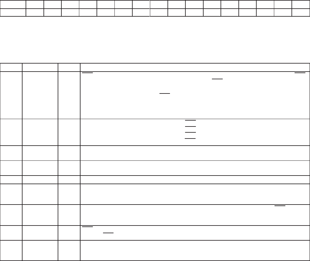
Bit 15 14 13 12 11 10 9 8 7 6 5 4 3 2 1 0
Default 1 1 1 1 1 1 1 0 0 0 0 1 0 0 1 0
Register: Power-management capabilities
Offset: A2h
Type: Read/Write, Read-only
Default: FE12h
Table 4−13. Power-Management Capabilities Register Description
BIT SIGNAL TYPE FUNCTION
PME support. This 5-bit field indicates the power states from which the controller function may assert PME.
A 0b for any bit indicates that the function cannot assert the PME
signal while in that power state. These
five bits return 11111b when read. Each of these bits is described below:
15 PME_Suppor
t
RW
Bit 15 defaults to 1b indicating the PME signal can be asserted from the D3
cold
state. This bit is R/W
because wake-up support from D3
cold
is contingent on the system providing an auxiliary power source to
the V
CC
terminals. If the system designer chooses not to provide an auxiliary power source to the V
CC
terminals for D3
cold
wake-up support, then BIOS should write a 0b to this bit.
14−11 PME_Support R
Bit 14 contains the value 1b, indicating that the PME signal can be asserted from D3
hot
state.
Bit 13 contains the value 1b, indicating that the PME
signal can be asserted from D2 state.
Bit 12 contains the value 1b, indicating that the PME
signal can be asserted from D1 state.
Bit 11 contains the value 1b, indicating that the PME
signal can be asserted from the D0 state.
10 D2_Support R
D2 support. Bit 10 returns a 1b when read, indicating that the CardBus function supports the D2 device
power state.
9 D1_Support R
D1 support. Bit 9 returns a 1b when read, indicating that the CardBus function supports the D1 device
power state.
8−6 RSVD R Reserved. Bits 8−6 return 000b when read.
5 DSI R
Device-specific initialization. Bit 5 returns 1b when read, indicating that the CardBus controller function
requires special initialization (beyond the standard PCI configuration header) before the generic-class
device driver is able to use it.
4 AUX_PWR R
Auxiliary power source. Bit 4 is tied to bit 15. When bit 4 is set, it indicates that support for PME in D3
cold
requires auxiliary power supplied by the system by way of a proprietary delivery vehicle. When bit 4 is 0b,
it indicates that the function supplies its own auxiliary power source.
3 PMECLK R
PME clock. Bit 3 returns 0b when read, indicating that no host bus clock is required for the controller to
generate PME
.
2−0 VERSION R
Version. Bits 2−0 return 010b when read, indicating that the power-management registers (PCI offsets
A4h−A7h, see Sections 4.38−4.40) are defined in the PCI Bus Power Management Interface Specification
version 1.1.
PREVIOUS2021222324252627282930313233NEXT