Freelance Electronics Components Distributor
Closed Dec 25th-26th
800-300-1968
We Stock Hard to Find Parts

PCI1510GGU

Part # PCI1510GGU
Description PCI TO PC CARD CONTROLLER - Trays
Category IC
Availability Out of Stock
Qty 0
Qty Price
1 + $3.74600


Technical Document


DISCLAIMER: The information provided herein is solely for informational purposes. Customers must be aware of the suitability of this product for their application, and consider that variable factors such as Manufacturer, Product Category, Date Codes, Pictures and Descriptions may differ from available inventory.

4−7
4.14 Secondary Status Register
The secondary status register is compatible with the PCI-to-PCI bridge secondary status register and indicates
CardBus-related device information to the host system. This register is very similar to the status register (offset 06h,
see Section 4.5); status bits are cleared by writing a 1b. See Table 4−5 for a complete description of the register
contents.
Bit 15 14 13 12 11 10 9 8 7 6 5 4 3 2 1 0
Default 0 0 0 0 0 0 1 0 0 0 0 0 0 0 0 0
Register: Secondary status
Offset: 16h
Type: Read-only, Read/Clear
Default: 0200h
Table 4−5. Secondary Status Register Description
BIT SIGNAL TYPE FUNCTION
15 CBPARITY RC Detected parity error. Bit 15 is set when a CardBus parity error is detected (either address or data).
14 CBSERR RC
Signaled system error. Bit 14 is set when CSERR is signaled by a CardBus card. The controller does not
assert CSERR
.
13 CBMABORT RC
Received master abort. Bit 13 is set when a cycle initiated by the controller on the CardBus bus has been
terminated by a master abort.
12 REC_CBTA RC
Received target abort. Bit 12 is set when a cycle initiated by the controller on the CardBus bus is terminated
by a target abort.
11 SIG_CBTA RC
Signaled target abort. Bit 11 is set by the controller when it terminates a transaction on the CardBus bus
with a target abort.
10−9 CB_SPEED R
CDEVSEL timing. These bits encode the timing of CDEVSEL and are hardwired 01b, indicating that the
controller asserts CB_SPEED at a medium speed.
8 CB_DPAR RC
CardBus data parity error detected.
0 = The conditions for setting bit 8 have not been met.
1 = A data parity error occurred and the following conditions were met:
a. CPERR
was asserted on the CardBus interface.
b. The controller was the bus master during the data parity error.
c. The parity error response bit is set in the bridge control.
7 CBFBB_CAP R
Fast back-to-back capable. The controller cannot accept fast back-to-back transactions; therefore, bit 7
is hardwired to 0b.
6 CB_UDF R
User-definable feature support. The controller does not support user-definable features; therefore, bit 6
is hardwired to 0b.
5 CB66MHZ R
66-MHz capable. The CardBus interface operates at a maximum CCLK frequency of 33 MHz; therefore,
bit 5 is hardwired to 0b.
4−0 RSVD R Reserved. Bits 4−0 return 00000b when read.
4−8
4.15 PCI Bus Number Register
This register is programmed by the host system to indicate the bus number of the PCI bus to which the controller is
connected. The controller uses this register in conjunction with the CardBus bus number and subordinate bus number
registers to determine when to forward PCI configuration cycles to its secondary buses.
Bit 7 6 5 4 3 2 1 0
Default 0 0 0 0 0 0 0 0
Register: PCI bus number
Offset: 18h
Type: Read/Write
Default: 00h
4.16 CardBus Bus Number Register
This register is programmed by the host system to indicate the bus number of the CardBus bus to which the controller
is connected. The controller uses this register in conjunction with the PCI bus number and subordinate bus number
registers to determine when to forward PCI configuration cycles to its secondary buses.
Bit 7 6 5 4 3 2 1 0
Default 0 0 0 0 0 0 0 0
Register: CardBus bus number
Offset: 19h
Type: Read/Write
Default: 00h
4.17 Subordinate Bus Number Register
This register is programmed by the host system to indicate the highest-numbered bus below the CardBus bus. The
controller uses this register in conjunction with the PCI bus number and CardBus bus number registers to determine
when to forward PCI configuration cycles to its secondary buses.
Bit 7 6 5 4 3 2 1 0
Default 0 0 0 0 0 0 0 0
Register: Subordinate bus number
Offset: 1Ah
Type: Read/Write
Default: 00h
4.18 CardBus Latency Timer Register
This register is programmed by the host system to specify the latency timer for the CardBus interface in units of CCLK
cycles. When the controller is a CardBus initiator and asserts CFRAME
, the CardBus latency timer begins counting.
If the latency timer expires before the transaction has terminated, then the controller terminates the transaction at
the end of the next data phase. A recommended minimum value for this register is 40h, which allows most
transactions to be completed.
Bit 7 6 5 4 3 2 1 0
Default 0 0 0 0 0 0 0 0
Register: CardBus latency timer
Offset: 1Bh
Type: Read/Write
Default: 00h
4−9
4.19 Memory Base Registers 0, 1
The memory base registers indicate the lower address of a PCI memory address range. These registers are used
by the controller to determine when to forward a memory transaction to the CardBus bus and when to forward a
CardBus cycle to PCI. Bits 31−12 of these registers are read/write and allow the memory base to be located anywhere
in the 32-bit PCI memory space on 4-Kbyte boundaries. Bits 11−0 are read-only and always return 000h. Write
transactions to these bits have no effect. Bits 8 and 9 of the bridge control register specify whether memory windows
0 and 1 are prefetchable or nonprefetchable. The memory base register or the memory limit register must be nonzero
for the controller to claim any memory transactions through CardBus memory windows (that is, these windows are
not enabled by default to pass the first 4 Kbytes of memory to CardBus).
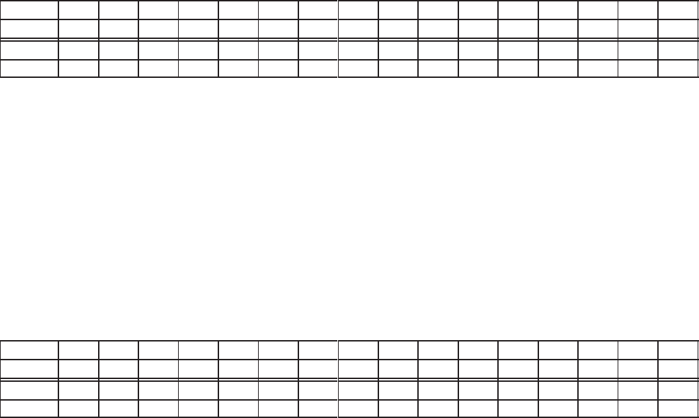
Bit 31 30 29 28 27 26 25 24 23 22 21 20 19 18 17 16
Default 0 0 0 0 0 0 0 0 0 0 0 0 0 0 0 0
Bit 15 14 13 12 11 10 9 8 7 6 5 4 3 2 1 0
Default 0 0 0 0 0 0 0 0 0 0 0 0 0 0 0 0
Register: Memory base registers 0, 1
Offset: 1Ch, 24h
Type: Read-only, Read/Write
Default: 0000 0000h
4.20 Memory Limit Registers 0, 1
The memory limit registers indicate the upper address of a PCI memory address range. These registers are used
by the controller to determine when to forward a memory transaction to the CardBus bus and when to forward a
CardBus cycle to PCI. Bits 31−12 of these registers are read/write and allow the memory base to be located anywhere
in the 32-bit PCI memory space on 4-Kbyte boundaries. Bits 11−0 are read-only and always return 000h. Write
transactions to these bits have no effect. Bits 8 and 9 of the bridge control register specify whether memory windows
0 and 1 are prefetchable or nonprefetchable. The memory base register or the memory limit register must be nonzero
for the controller to claim any memory transactions through CardBus memory windows; that is, these windows are
not enabled by default to pass the first 4 Kbytes of memory to CardBus.
Bit 31 30 29 28 27 26 25 24 23 22 21 20 19 18 17 16
Default 0 0 0 0 0 0 0 0 0 0 0 0 0 0 0 0
Bit 15 14 13 12 11 10 9 8 7 6 5 4 3 2 1 0
Default 0 0 0 0 0 0 0 0 0 0 0 0 0 0 0 0
Register: Memory limit registers 0, 1
Offset: 20h, 28h
Type: Read-only, Read/Write
Default: 0000 0000h
PREVIOUS1617181920212223242526272829NEXT