Closed Dec 25th-26th
800-300-1968
We Stock Hard to Find Parts
My Account
|
My Orders
|
My Cart
Questions?
(800) 300-1968
Register
(current)
My Account
(current)
My Orders
(current)
My Cart
(current)
Categories
(current)
Manufacturers
Request a Quote
Sell Your Excess
Consignment
Quality Assurance
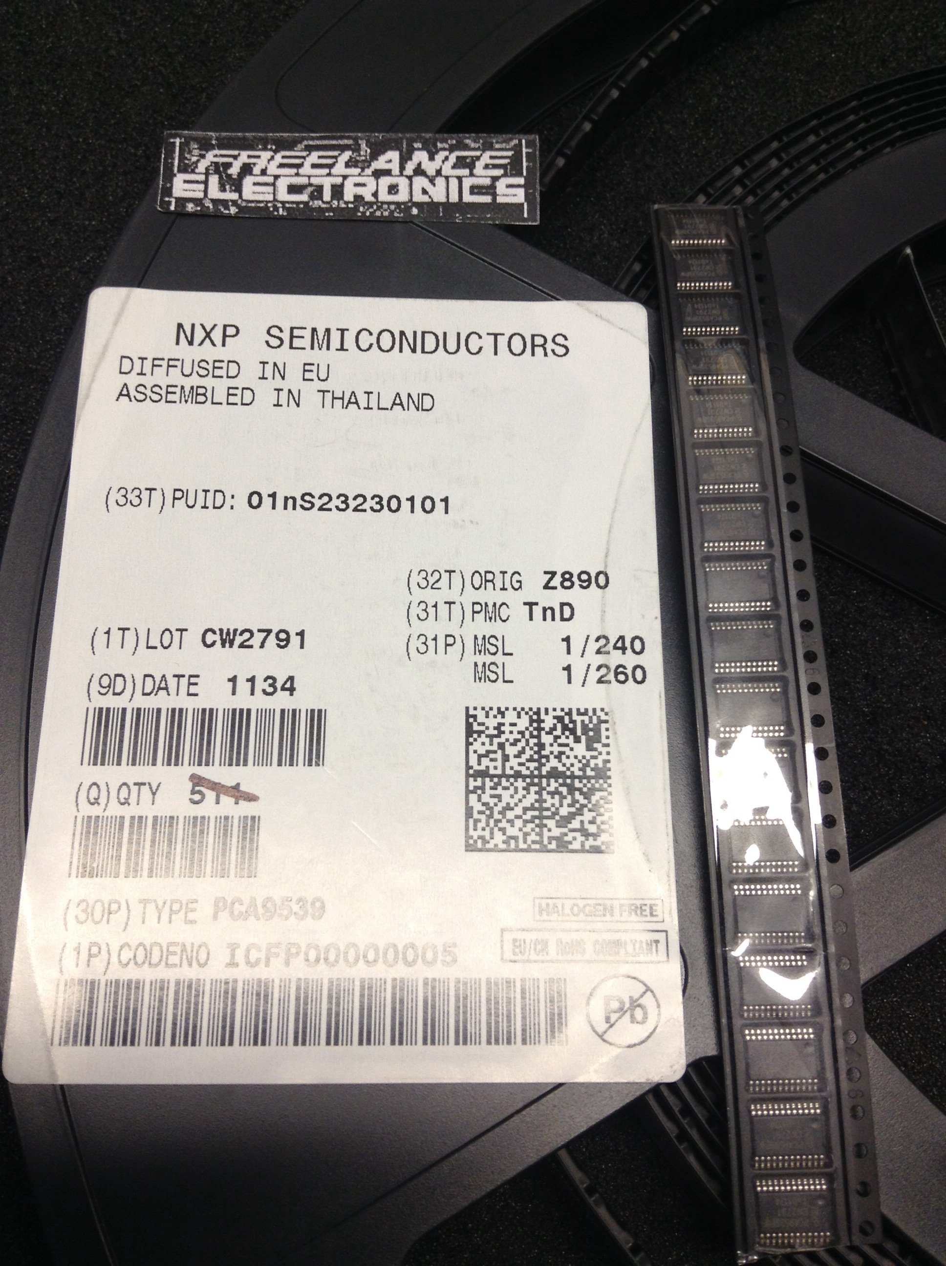
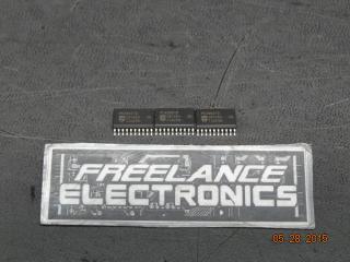
PCA9539PW
Part #
PCA9539PW
Description
IC DB,DBQ,DGV,DW,PW,RHL,RGE - Rail/Tube
Category
IC
Availability
Out of Stock
Qty
0
Qty
Price
1 +
$1.54520
Related Items
NXP SEMICONDUCTORS
IC
PCA9500BS,118
$0.61371
NXP SEMICONDUCTORS
IC
PCA9500BSHP
$7.58541
Philips Semiconductor
IC
PCA9501BS
$9.25193
Philips Semiconductor
IC
PCA9501D
$5.97361
Philips Semiconductor
IC
PCA9504ADGG
$2.58731
Philips Semiconductor
IC
PCA9506DGG
$15.74144