OPA604
12
SBOS019A
www.ti.com
1
0
01
I
C
(mA)
05
log
(V
O
)
1234
f
O
2f
O
3f
O
4f
O
5f
O
V
BE
= 1kHz + DC Bias
V
BE
(V)
0.65
FFT
Frequency (kHz)
1
0
10
–I
D
(mA)
05
log
(V
O
)
1234
f
O
2f
O
3f
O
4f
O
5f
O
V
GS
= 1kHz + DC Bias
V
GS
(V)
FFT
Frequency (kHz)
V
O
I
D
V
GS
V
O
I
C
V
BE
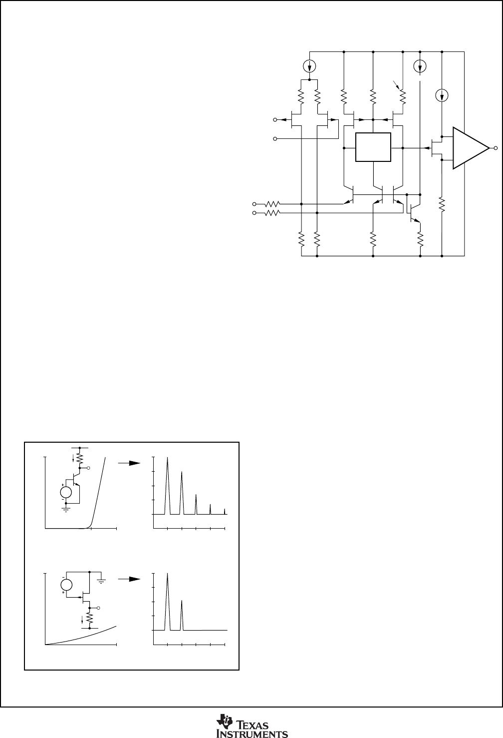
FIGURE 10. I-V and Spectral Response of NPN and
JFET.
THE OPA604 DESIGN
The OPA604 uses FETs throughout the signal path,
including the input stage, input-stage load, and the
important phase-splitting section of the output stage.
Bipolar transistors are used where their attributes,
such as current capability are important, and where
their transfer characteristics have minimal impact.
The topology consists of a single folded-cascode gain
stage followed by a unity-gain output stage. Differen-
tial input transistors J
1
and J
2
are special large-geom-
etry, P-channel JFETs. Input stage current is a rela-
tively high 800µA, providing high transconductance
and reducing voltage noise. Laser trimming of stage
currents and careful attention to symmetry yields a
nearly symmetrical slew rate of ±25V/µs.
The JFET input stage holds input bias current to
approximately 50pA or roughly 3000 times lower than
common bipolar-input audio op amps. This dramati-
cally reduces noise with high-impedance circuitry.
The drains of J
1
and J
2
are cascoded by Q
1
and Q
2
,
driving the input stage loads, FETs J
3
and J
4
. Distor-
tion reduction circuitry (patented) linearizes the open-
loop response and increases voltage gain. The 20MHz
bandwidth of the OPA604 further reduces distortion
through the user-connected feedback loop.
The output stage consists of a JFET phase-splitter
loaded into high speed all-NPN output drivers. Output
transistors are biased by a special circuit to prevent
cutoff, even with full output swing into 600Ω loads.
The following discussion is provided, recognizing that
not all measured performance behavior explains or
correlates with listening tests by audio experts. The
design of the OPA604 included consideration of both
objective performance measurements, as well as an
awareness of widely held theory on the success and
failure of previous op amp designs.
SOUND QUALITY
The sound quality of an op amp is often the crucial
selection criteria—even when a data sheet claims
exceptional distortion performance. By its nature, sound
quality is subjective. Furthermore, results of listening
tests can vary depending on application and circuit
configuration. Even experienced listeners in controlled
tests often reach different conclusions.
Many audio experts believe that the sound quality of a
high performance FET op amp is superior to that of
bipolar op amps. A possible reason for this is that
bipolar designs generate greater odd-order harmonics
than FETs. To the human ear, odd-order harmonics
have long been identified as sounding more unpleas-
ant than even-order harmonics. FETs, like vacuum
tubes, have a square-law I-V transfer function which is
more linear than the exponential transfer function of a
bipolar transistor. As a direct result of this square-law
characteristic, FETs produce predominantly even-or-
der harmonics. Figure 10 shows the transfer function of
a bipolar transistor and FET. Fourier transformation of
both transfer functions reveals the lower odd-order
harmonics of the FET amplifier stage.
SOUND QUALITY
Distortion
Rejection
Circuitry
(+)
(–)
Output
Stage
R
3
1kΩ
R
4
1kΩ
R
8
3kΩ
R
9
3kΩ
R
1
75Ω
R
2
75Ω
R
5
500Ω
R
7
4kΩ
R
6
500Ω
I
1
800µA
J
1
J
2
J
3
J
4
Q
4
Q
2
Q
3
Q
1
J
5
I
2
200µA
R
10
10kΩ
R
11
10kΩ


