Freelance Electronics Components Distributor
Closed Dec 25th-26th
800-300-1968
We Stock Hard to Find Parts

OPA604AP

Part # OPA604AP
Description FET INPUT AUDIO OP AMP - Rail/Tube
Category IC
Availability In Stock
Qty 1
Qty Price
1 + $1.67469
Manufacturer Available Qty
Burr-Brown Corporation
Date Code: 9241
  • Shipping Freelance Stock: 1
    Ships Immediately


Technical Document


DISCLAIMER: The information provided herein is solely for informational purposes. Customers must be aware of the suitability of this product for their application, and consider that variable factors such as Manufacturer, Product Category, Date Codes, Pictures and Descriptions may differ from available inventory.

FEATURES
LOW DISTORTION: 0.0003% at 1kHz
LOW NOISE: 10nV/Hz
HIGH SLEW RATE: 25V/µs
WIDE GAIN-BANDWIDTH: 20MHz
UNITY-GAIN STABLE
WIDE SUPPLY RANGE: V
S
= ±4.5 to ±24V
DRIVES 600 LOAD
DUAL VERSION AVAILABLE (OPA2604)
FET-Input, Low Distortion
OPERATIONAL AMPLIFIER
APPLICATIONS
PROFESSIONAL AUDIO EQUIPMENT
PCM DAC I/V CONVERTERS
SPECTRAL ANALYSIS EQUIPMENT
ACTIVE FILTERS
TRANSDUCER AMPLIFIERS
DATA ACQUISITION
OPA604
DESCRIPTION
The OPA604 is a FET-input operational amplifier designed
for enhanced AC performance. Very low distortion, low noise
and wide bandwidth provide superior performance in high
quality audio and other applications requiring excellent dy-
namic performance.
New circuit techniques and special laser trimming of dynamic
circuit performance yield very low harmonic distortion. The
result is an op amp with exceptional sound quality. The low-
noise FET input of the OPA604 provides wide dynamic
range, even with high source impedance. Offset voltage is
laser-trimmed to minimize the need for interstage coupling
capacitors.
The OPA604 is available in 8-pin plastic mini-DIP and SO-8
surface-mount packages, specified for the –25°C to +85°C
temperature range.
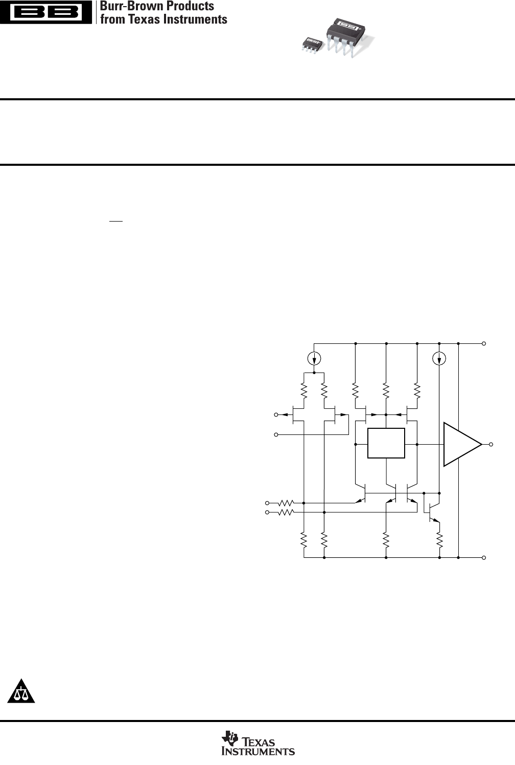
Distortion
Rejection
Circuitry
(1)
(3)
(+)
(2)
()
(7)
V+
(6)
V
O
(4)
V
Output
Stage
(1)
NOTE: (1) Patents Granted: #5053718, 5019789
(5)
(1)
O
P
A
6
0
4
O
P
A
6
0
4
SBOS019A JANUARY 1992 SEPTEMBER 2003
www.ti.com
PRODUCTION DATA information is current as of publication date.
Products conform to specifications per the terms of Texas Instruments
standard warranty. Production processing does not necessarily include
testing of all parameters.
Copyright © 1992-2003, Texas Instruments Incorporated
Please be aware that an important notice concerning availability, standard warranty, and use in critical applications of
Texas Instruments semiconductor products and disclaimers thereto appears at the end of this data sheet.
All trademarks are the property of their respective owners.
OPA604
2
SBOS019A
www.ti.com
ABSOLUTE MAXIMUM RATINGS
Power Supply Voltage ....................................................................... ±25V
Input Voltage ............................................................... (V)1V to (V+)+1V
Output Short Circuit to Ground ................................................ Continuous
Operating Temperature .................................................. 40°C to +100°C
Storage Temperature ...................................................... 40°C to +125°C
Junction Temperature .................................................................... +150°C
Lead Temperature (soldering, 10s) AP .......................................... +300°C
Lead Temperature (soldering, 3s) AU............................................ +260°C
PIN CONFIGURATION
Top View DIP, SOIC
1
2
3
4
Offset Trim
In
+In
V
S
8
7
6
5
No Internal Connection
+V
S
Output
Offset Trim
ELECTROSTATIC
DISCHARGE SENSITIVITY
Any integrated circuit can be damaged by ESD. Texas Instru-
ments recommends that all integrated circuits be handled with
appropriate precautions. Failure to observe proper handling
and installation procedures can cause damage.
ESD damage can range from subtle performance degradation
to complete device failure. Precision integrated circuits may be
more susceptible to damage because very small parametric
changes could cause the device not to meet published speci-
fications.
PACKAGE/ORDERING INFORMATION
For the most current package and ordering information, see
to the Package Option Addendum at the end of this data
sheet.
OPA604
3
SBOS019A
www.ti.com
ELECTRICAL CHARACTERISTICS
T
A
= +25°C, V
S
= ±15V, unless otherwise noted.
OPA604AP, AU
PARAMETER CONDITION MIN TYP MAX UNITS
OFFSET VOLTAGE
Input Offset Voltage ±1 ±5mV
Average Drift ±8 µV/°C
Power Supply Rejection V
S
= ±5 to ±24V 80 100 dB
INPUT BIAS CURRENT
(1)
Input Bias Current V
CM
= 0V 50 pA
Input Offset Current V
CM
= 0V ±3pA
NOISE
Input Voltage Noise
Noise Density: f = 10Hz 25 nV/Hz
f = 100Hz 15 nV/Hz
f = 1kHz 11 nV/Hz
f = 10kHz 10 nV/Hz
Voltage Noise, BW = 20Hz to 20kHz 1.5 µV
PP
Input Bias Current Noise
Current Noise Density, f = 0.1Hz to 20kHz 4fA/Hz
INPUT VOLTAGE RANGE
Common-Mode Input Range ±12 ±13 V
Common-Mode Rejection V
CM
= ±12V 80 100 dB
INPUT IMPEDANCE
Differential 10
12
|| 8 || pF
Common-Mode 10
12
|| 10 || pF
OPEN-LOOP GAIN
Open-Loop Voltage Gain V
O
= ±10V, R
L
= 1k 80 100 dB
FREQUENCY RESPONSE
Gain-Bandwidth Product G = 100 20 MHz
Slew Rate 20V
PP
, R
L
= 1k 15 25 V/µs
Settling Time: 0.01% G = 1, 10V Step 1.5 µs
0.1% 1 µs
Total Harmonic Distortion + Noise (THD+N) G = 1, f = 1kHz 0.0003 %
V
O
= 3.5Vrms, R
L
= 1k
OUTPUT
Voltage Output R
L
= 600Ω±11 ±12 V
Current Output V
O
= ±12V ±35 mA
Short Circuit Current ±40 mA
Output Resistance, Open-Loop 25
POWER SUPPLY
Specified Operating Voltage ±15 V
Operating Voltage Range ±4.5 ±24 V
Current ±5.3 ±7mA
TEMPERATURE RANGE
Specification 25 +85 °C
Storage 40 +125 °C
Thermal Resistance
(2)
,
θ
JA
90 °C/W
NOTES: (1) Typical performance, measured fully warmed-up. (2) Soldered to circuit boardsee text.
123456NEXT