Freelance Electronics Components Distributor
Closed Dec 25th-26th
800-300-1968
We Stock Hard to Find Parts

OPA4348AIDG4

Part # OPA4348AIDG4
Description IC OPAMP GP 1MHZ RRO 14SOIC
Category IC
Availability In Stock
Qty 105
Qty Price
1 - 22 $1.26509
23 - 44 $1.00632
45 - 66 $0.94882
67 - 88 $0.88173
89 + $0.78589
Manufacturer Available Qty
Texas Instruments
  • Shipping Freelance Stock: 5
    Ships Immediately
Texas Instruments
  • Shipping Freelance Stock: 100
    Ships Immediately


Technical Document


DISCLAIMER: The information provided herein is solely for informational purposes. Customers must be aware of the suitability of this product for their application, and consider that variable factors such as Manufacturer, Product Category, Date Codes, Pictures and Descriptions may differ from available inventory.

OPA348, 2348, 4348
7
SBOS213C
www.ti.com
FIGURE 3. OPA348No Phase Inversion with Inputs Greater
than the Power-Supply Voltage.
APPLICATIONS INFORMATION
OPA348 series op amps are unity-gain stable and suitable
for a wide range of general-purpose applications.
The OPA348 series features wide bandwidth and unity-gain
stability with rail-to-rail input and output for increased dynamic
range. Figure 1 shows the input and output waveforms for the
OPA348 in unity-gain configuration. Operation is from a single
+5V supply with a 100k load connected to V
S
/2. The input is
a 5Vp-p sinusoid. Output voltage is approximately 4.98Vp-p.
Power-supply pins should be bypassed with 0.01µF ceramic
capacitors.
on the high end. Within the 200mV transition region PSRR,
CMRR, offset voltage, offset drift, and THD may be degraded
compared to operation outside this region.
FIGURE 1. The OPA348 Features Rail-to-Rail Input/Output.
5V
1V/div
0V
G = +1V/V, V
S
= +5V
20µs/div
Output (Inverted on Scope)
OPERATING VOLTAGE
OPA348 series op amps are fully specified and tested from
+2.5V to +5.5V. However, supply voltage may range from
+2.1V to +5.5V. Parameters are tested over the specified
supply rangea unique feature of the OPA348 series. In
addition, all temperature specifications apply from 40°C to
+125°C. Most behavior remains virtually unchanged through-
out the full operating voltage range. Parameters that vary
significantly with operating voltages or temperature are shown
in the Typical Characteristics.
COMMON-MODE VOLTAGE RANGE
The input common-mode voltage range of the OPA348 series
extends 200mV beyond the supply rails. This is achieved
with a complementary input stagean N-channel input differ-
ential pair in parallel with a P-channel differential pair. The
N-channel pair is active for input voltages close to the positive
rail, typically (V+) 1.2V to 300mV above the positive supply,
while the P-channel pair is on for inputs from 300mV below the
negative supply to approximately (V+) 1.4V. There is a small
transition region, typically (V+) 1.4V to (V+) 1.2V, in which
both pairs are on. This 200mV transition region, shown in
Figure 2, can vary ±300mV with process variation. Thus, the
transition region (both stages on) can range from (V+) 1.7V
to (V+) 1.5V on the low end, up to (V+) 1.1V to (V+) 0.9V
RAIL-TO-RAIL INPUT
The input common-mode range extends from (V) 0.2V to
(V+) + 0.2V. For normal operation, inputs should be limited to
this range. The absolute maximum input voltage is 500mV
beyond the supplies. Inputs greater than the input common-
mode range but less than the maximum input voltage, while not
valid, will not cause any damage to the op amp. Unlike some
other op amps, if input current is limited the inputs may go
beyond the power supplies without phase inversion, as shown
in Figure 3.
5V
1V/div
0V
G = +1V/V, V
S
= +5V
10µs/div
V
IN
V
OUT
FIGURE 2. Behavior of Typical Transition Region at Room
Temperature.
OPA348, 2348, 4348
8
SBOS213C
www.ti.com
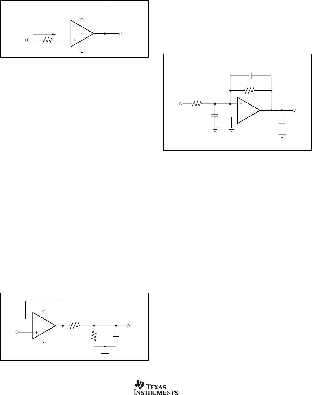
In unity-gain inverter configuration, phase margin can be
reduced by the reaction between the capacitance at the op
amp input, and the gain setting resistors, thus degrading
capacitive load drive. Best performance is achieved by using
small valued resistors. For example, when driving a 500pF
load, reducing the resistor values from 100k to 5k de-
creases overshoot from 55% to 13% (see the typical charac-
teristic Small-Signal Overshoot vs. Load Capacitance).
However, when large valued resistors cannot be avoided, a
small (4pF to 6pF) capacitor, C
FB
, can be inserted in the
feedback, as shown in Figure 6. This significantly reduces
overshoot by compensating the effect of capacitance, C
IN
,
which includes the amplifier's input capacitance and PC
board parasitic capacitance.
FIGURE 6. Improving Capacitive Load Drive.
Normally, input currents are 0.5pA. However, large inputs
(greater than 500mV beyond the supply rails) can cause
excessive current to flow in or out of the input pins. There-
fore, as well as keeping the input voltage below the maxi-
mum rating, it is also important to limit the input current to
less than 10mA. This is easily accomplished with an input
voltage resistor, as shown in Figure 4.
R
I
OPA348
V
IN
V
OUT
R
F
C
FB
C
IN
C
L
FIGURE 4. Input Current Protection for Voltages Exceeding
the Supply Voltage.
5k
OPA348
10mA max
+5V
V
IN
V
OUT
I
OVERLOAD
RAIL-TO-RAIL OUTPUT
A class AB output stage with common-source transistors is
used to achieve rail-to-rail output. This output stage is ca-
pable of driving 5k loads connected to any potential be-
tween V+ and ground. For light resistive loads (> 100k), the
output voltage can typically swing to within 18mV from supply
rail. With moderate resistive loads (10k to 50k), the output
voltage can typically swing to within 100mV of the supply
rails while maintaining high open-loop gain (see the typical
characteristic Output Voltage Swing vs Output Current).
CAPACITIVE LOAD AND STABILITY
The OPA348 in a unity-gain configuration can directly drive
up to 250pF pure capacitive load. Increasing the gain en-
hances the amplifiers ability to drive greater capacitive loads
(see the typical characteristic Small-Signal Overshoot vs
Capacitive Load). In unity-gain configurations, capacitive
load drive can be improved by inserting a small (10 to 20)
resistor, R
S
, in series with the output, as shown in Figure 5.
This significantly reduces ringing while maintaining DC per-
formance for purely capacitive loads. However, if there is a
resistive load in parallel with the capacitive load, a voltage
divider is created, introducing a Direct Current (DC) error at
the output and slightly reducing the output swing. The error
introduced is proportional to the ratio R
S
/R
L
, and is generally
negligible.
FIGURE 5. Series Resistor in Unity-Gain Buffer Configura-
tion Improves Capacitive Load Drive.
10to
20
OPA348
V+
V
IN
V
OUT
R
S
R
L
C
L
DRIVING A/D CONVERTERS
The OPA348 series op amps are optimized for driving
medium-speed sampling Analog-to-Digital Converters (ADCs).
The OPA348 op amps buffer the ADCs input capacitance
and resulting charge injection while providing signal gain.
The OPA348 in a basic noninverting configuration driving the
ADS7822, see Figure 7. The ADS7822 is a 12-bit,
micro
POWER sampling converter in the MSOP-8 package.
When used with the low-power, miniature packages of the
OPA348, the combination is ideal for space-limited, low-
power applications. In this configuration, an RC network at
the ADCs input can be used to provide for anti-aliasing filter
and charge injection current.
The OPA348 in noninverting configuration driving ADS7822
limited, low-power applications. In this configuration, an RC
network at the ADCs input can be used to provide for anti-
aliasing filter and charge injection current. See Figure 8 for
the OPA2348 driving an ADS7822 in a speech bandpass
filtered data acquisition system. This small, low-cost solution
provides the necessary amplification and signal conditioning
to interface directly with an electret microphone. This circuit
will operate with V
S
= 2.7V to 5V with less than 250µA typical
quiescent current.
OPA348, 2348, 4348
9
SBOS213C
www.ti.com
FIGURE 8. OPA2348 as a Speech Bandpass Filtered Data Acquisition System.
FIGURE 7. OPA348 in Noninverting Configuration Driving ADS7822.
ADS7822
12-Bit A/D
DCLOCK
D
OUT
CS/SHDN
OPA348
+5V
V
IN
V+
2
+In
3
In
V
REF
8
4GND
Serial
Interface
1
0.1µF 0.1µF
7
6
5
NOTE: A/D Input = 0 to V
REF
V
IN
= 0V to 5V for
0V to 5V output.
RC network filters high frequency noise.
500
3300pF
C
3
33pF
V
+
GND
3
1
8
4
5
6
7
IN
+IN
2
C
2
DCLOCK
Serial
Interface
1000pF
R
1
1.5k
R
4
20k
R
5
20k
R
6
100k
R
8
150k
R
9
510k
R
7
51k
D
OUT
V
REF
V+
= +2.7V to 5V
CS/SHDN
C
1
1000pF
Electret
Microphone
(1)
G = 100
Passband 300Hz to 3kHz
R
3
1M
R
2
1M
NOTE: (1) Electret microphone
powered by R
1
.
ADS7822
12-Bit A/D
1/2
OPA2348
1/2
OPA2348
PREVIOUS123456NEXT