Freelance Electronics Components Distributor
Closed Dec 25th-26th
800-300-1968
We Stock Hard to Find Parts

OPA177GP

Part # OPA177GP
Description Precision Operational Amplifier
Category IC
Availability Out of Stock
Qty 0
Qty Price
1 + $1.13930


Technical Document


DISCLAIMER: The information provided herein is solely for informational purposes. Customers must be aware of the suitability of this product for their application, and consider that variable factors such as Manufacturer, Product Category, Date Codes, Pictures and Descriptions may differ from available inventory.

7
®
OPA177
APPLICATIONS INFORMATION
The OPA177 is unity-gain stable, making it easy to use and
free from oscillations in the widest range of circuitry. Ap-
plications with noisy or high impedance power supply lines
may require decoupling capacitors close to the device pins.
In most cases 0.1µF ceramic capacitors are adequate.
The OPA177 has very low offset voltage and drift. To
achieve highest performance, circuit layout and mechanical
conditions must be optimized. Offset voltage and drift can
be degraded by small thermoelectric potentials at the op amp
inputs. Connections of dissimilar metals will generate ther-
mal potential which can mask the ultimate performance of
the OPA177. These thermal potentials can be made to cancel
by assuring that they are equal in both input terminals.
1. Keep connections made to the two input terminals close
together.
2. Locate heat sources as far as possible from the critical
input circuitry.
3. Shield the op amp and input circuitry from air currents
such as cooling fans.
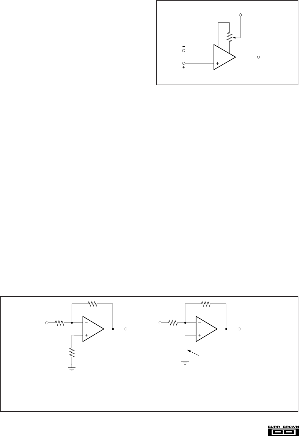
OFFSET VOLTAGE ADJUSTMENT
The OPA177 has been laser-trimmed for low offset voltage
and drift so most circuits will not require external adjust-
ment. Figure 1 shows the optional connection of an external
potentiometer to adjust offset voltage. This adjustment should
not be used to compensate for offsets created elsewhere in a
system since this can introduce excessive temperature drift.
INPUT PROTECTION
The inputs of the OPA177 are protected with 500 series
input resistors and diode clamps as shown in the simplified
circuit diagram. The inputs can withstand ±30V differential
inputs without damage. The protection diodes will, of course,
conduct current when the inputs are overdriven. This may
disturb the slewing behavior of unity-gain follower applica-
tions, but will not damage the op amp.
NOISE PERFORMANCE
The noise performance of the OPA177 is optimized for
circuit impedances in the range of 2k to 50k. Total noise
in an application is a combination of the op amp’s input
voltage noise and input bias current noise reacting with
circuit impedances. For applications with higher source
impedance, the OPA627 FET-input op amp will generally
provide lower noise. For very low impedance applications,
the OPA27 will provide lower noise.
INPUT BIAS CURRENT CANCELLATION
The input stage base current of the OPA177 is internally
compensated with an equal and opposite cancellation cur-
rent. The resulting input bias current is the difference
between the input stage base current and the cancellation
current. This residual input bias current can be positive or
negative.
When the bias current is cancelled in this manner, the input
bias current and input offset current are approximately the
same magnitude. As a result, it is not necessary to balance
the DC resistance seen at the two input terminals (Figure 2).
A resistor added to balance the input resistances may actu-
ally increase offset and noise.
FIGURE 1. Optional Offset Nulling Circuit.
OPA177
V
2
3
1
8
Trim Range is approximately ±3.0mV
V+
20k
OUT
V
IN
Op Amp
(a)
R
B
OPA177
(b)
No bias current
cancellation resistor needed
Conventional op amp with
external bias current
cancellation resistor.
OPA177 with no external
bias current cancellation
resistor.
= R
2
|| R
1
R
2
R
1
R
2
R
1
FIGURE 2. Input Bias Current Cancellation.
PACKAGING INFORMATION
Orderable Device Status
(1)
Package
Type
Package
Drawing
Pins Package
Qty
Eco Plan
(2)
Lead/Ball Finish MSL Peak Temp
(3)
OPA177FP ACTIVE PDIP P 8 50 Green (RoHS &
no Sb/Br)
CU NIPDAU N / A for Pkg Type
OPA177FPG4 ACTIVE PDIP P 8 50 Green (RoHS &
no Sb/Br)
CU NIPDAU N / A for Pkg Type
OPA177GP ACTIVE PDIP P 8 50 Green (RoHS &
no Sb/Br)
CU NIPDAU N / A for Pkg Type
OPA177GPG4 ACTIVE PDIP P 8 50 Green (RoHS &
no Sb/Br)
CU NIPDAU N / A for Pkg Type
OPA177GS ACTIVE SOIC D 8 75 Green (RoHS &
no Sb/Br)
CU NIPDAU Level-3-260C-168 HR
OPA177GS/2K5 ACTIVE SOIC D 8 2500 Green (RoHS &
no Sb/Br)
CU NIPDAU Level-3-260C-168 HR
OPA177GS/2K5E4 ACTIVE SOIC D 8 2500 Green (RoHS &
no Sb/Br)
CU NIPDAU Level-3-260C-168 HR
OPA177GS/2K5G4 ACTIVE SOIC D 8 2500 Green (RoHS &
no Sb/Br)
CU NIPDAU Level-3-260C-168 HR
OPA177GSE4 ACTIVE SOIC D 8 75 Green (RoHS &
no Sb/Br)
CU NIPDAU Level-3-260C-168 HR
OPA177GSG4 ACTIVE SOIC D 8 75 Green (RoHS &
no Sb/Br)
CU NIPDAU Level-3-260C-168 HR
(1)
The marketing status values are defined as follows:
ACTIVE: Product device recommended for new designs.
LIFEBUY: TI has announced that the device will be discontinued, and a lifetime-buy period is in effect.
NRND: Not recommended for new designs. Device is in production to support existing customers, but TI does not recommend using this part in
a new design.
PREVIEW: Device has been announced but is not in production. Samples may or may not be available.
OBSOLETE: TI has discontinued the production of the device.
(2)
Eco Plan - The planned eco-friendly classification: Pb-Free (RoHS), Pb-Free (RoHS Exempt), or Green (RoHS & no Sb/Br) - please check
http://www.ti.com/productcontent for the latest availability information and additional product content details.
TBD: The Pb-Free/Green conversion plan has not been defined.
Pb-Free (RoHS): TI's terms "Lead-Free" or "Pb-Free" mean semiconductor products that are compatible with the current RoHS requirements
for all 6 substances, including the requirement that lead not exceed 0.1% by weight in homogeneous materials. Where designed to be soldered
at high temperatures, TI Pb-Free products are suitable for use in specified lead-free processes.
Pb-Free (RoHS Exempt): This component has a RoHS exemption for either 1) lead-based flip-chip solder bumps used between the die and
package, or 2) lead-based die adhesive used between the die and leadframe. The component is otherwise considered Pb-Free (RoHS
compatible) as defined above.
Green (RoHS & no Sb/Br): TI defines "Green" to mean Pb-Free (RoHS compatible), and free of Bromine (Br) and Antimony (Sb) based flame
retardants (Br or Sb do not exceed 0.1% by weight in homogeneous material)
(3)
MSL, Peak Temp. -- The Moisture Sensitivity Level rating according to the JEDEC industry standard classifications, and peak solder
temperature.
Important Information and Disclaimer:The information provided on this page represents TI's knowledge and belief as of the date that it is
provided. TI bases its knowledge and belief on information provided by third parties, and makes no representation or warranty as to the
accuracy of such information. Efforts are underway to better integrate information from third parties. TI has taken and continues to take
reasonable steps to provide representative and accurate information but may not have conducted destructive testing or chemical analysis on
incoming materials and chemicals. TI and TI suppliers consider certain information to be proprietary, and thus CAS numbers and other limited
information may not be available for release.
In no event shall TI's liability arising out of such information exceed the total purchase price of the TI part(s) at issue in this document sold by TI
to Customer on an annual basis.
PACKAGE OPTION ADDENDUM
www.ti.com
16-Feb-2009
Addendum-Page 1
TAPE AND REEL INFORMATION
*All dimensions are nominal
Device Package
Type
Package
Drawing
Pins SPQ Reel
Diameter
(mm)
Reel
Width
W1 (mm)
A0 (mm) B0 (mm) K0 (mm) P1
(mm)
W
(mm)
Pin1
Quadrant
OPA177GS/2K5 SOIC D 8 2500 330.0 12.4 6.4 5.2 2.1 8.0 12.0 Q1
PACKAGE MATERIALS INFORMATION
www.ti.com
11-Mar-2008
Pack Materials-Page 1
PREVIOUS1234NEXT