Closed Dec 25th-26th
800-300-1968
We Stock Hard to Find Parts
My Account
|
My Orders
|
My Cart
Questions?
(800) 300-1968
Register
(current)
My Account
(current)
My Orders
(current)
My Cart
(current)
Categories
(current)
Manufacturers
Request a Quote
Sell Your Excess
Consignment
Quality Assurance
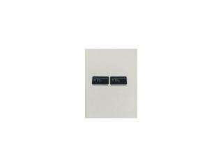
CY74FCT240ATSOC
Part #
CY74FCT240ATSOC
Description
Buffer/Line Driver 8-CH Inverting 3-ST CMOS 20-Pin SOIC Tu
Category
IC
Availability
In Stock
Qty
2
Qty
Price
1 +
$0.21370
Manufacturer
Available
Qty
CYPRESS SEMICONDUCTOR
Date Code: 9606
Freelance Stock:
2
Ships Immediately
Add to Cart
Related Items
CYPRESS SEMICONDUCTOR
IC
CY74FCT162245ATPAC
$4.82164
CYPRESS SEMICONDUCTOR
IC
CY74FCT162245ETPAC
$1.28020
CYPRESS SEMICONDUCTOR
IC
CY74FCT162245TPVC
$0.69768
CYPRESS SEMICONDUCTOR
IC
CY74FCT162373ATPAC
$1.02277
CYPRESS SEMICONDUCTOR
IC
CY74FCT162374ETPAC
$2.08536
CYPRESS SEMICONDUCTOR
IC
CY74FCT16245TPAC
$0.36527